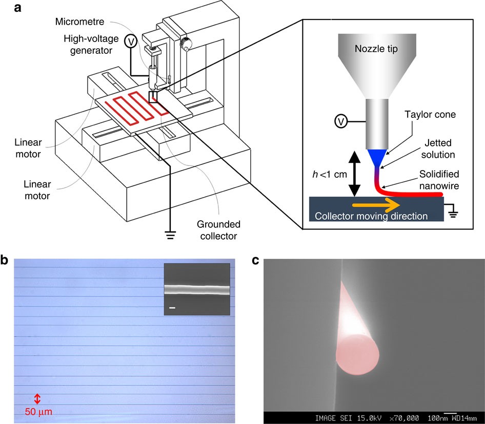
Figure 1: Organic nanowire printing.
From: Large-scale organic nanowire lithography and electronics

(a) Schematic diagram of ONW printer and NW printing process. (b) Optical micrograph of well-aligned PVK NWs. The diameter of PVK NW is 290 nm (inset, scale bar, 200 nm). (c) Field emission scanning electron microscope image showing cross section of well-aligned PVK NW, which forms a perfect circle.
