
Fig. 5: F(M) versus M for.
From: Infrared avalanche photodiodes from bulk to 2D materials
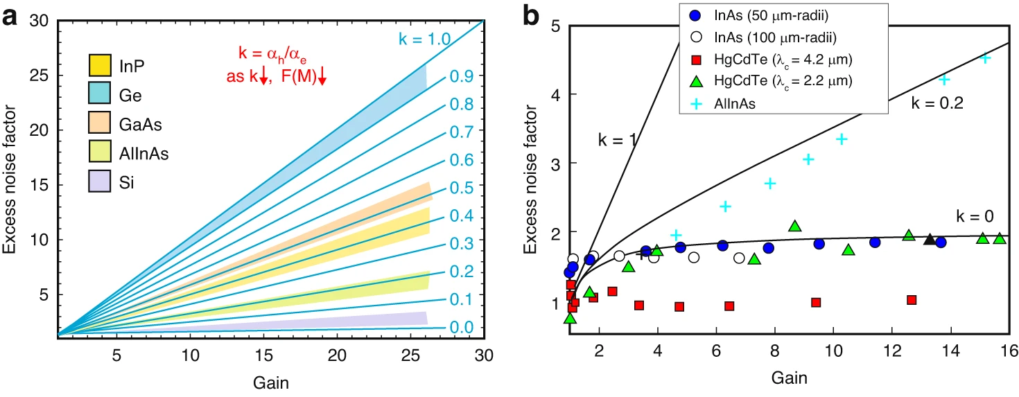
a Si, AlInAs, GaAs, Ge, InP [the solid lines present the F(M) for k within the range 0–1 (increment 0.1) calculated by the local field model24, typical F(M) are shown by shaded regions37 and b selected materials: 3.5 μm thick intrinsic InAs APDs (50 μm and 100 μm radius), 4.2 μm cut-off wavelengths HgCdTe and 2.2 μm InAlAs APDs134
