
Fig. 8: The device structure comparison between low-noise PMT and multi-quantum well APDs.
From: Infrared avalanche photodiodes from bulk to 2D materials
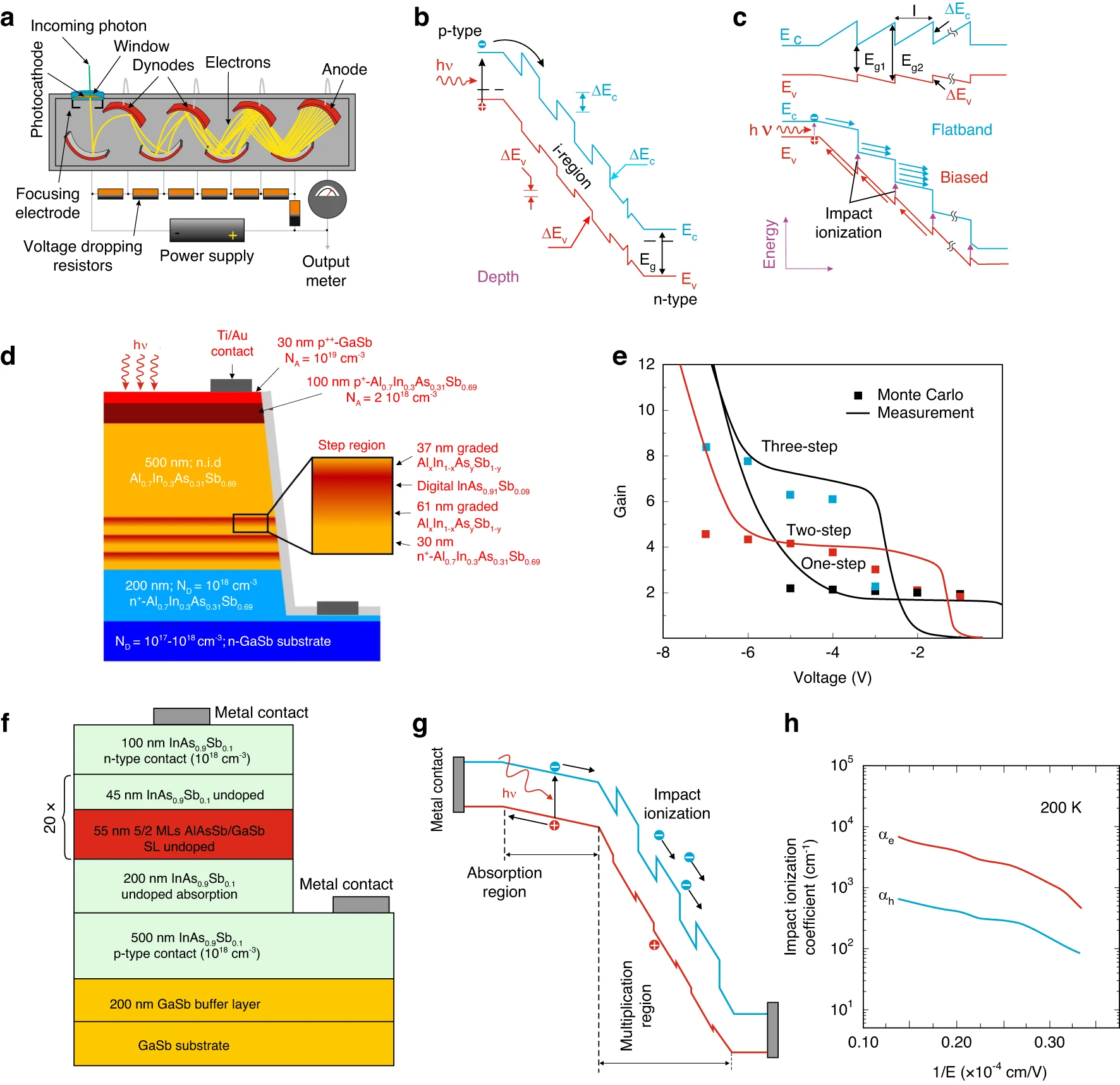
a schematic presentation of a photomultiplier tube, b multi-quantum well p-i-n APD energy band sketch with marked intrinsic region (i), c energy band profiles of staircase APD under zero (top) and reverse (bottom) voltage. Multistep AlInAsSb staircase avalanche photodiode: d 3-step staircase APD device profile, e theoretically calculated by Monte Carlo method and measured gain of 1-, 2-, and 3-stairs APDs for 300 K70. MWIR SAM-APD structure with AlAsSb/GaSb superlattice: f device design profile, g energy band structure under reverse voltage, and h carriers impact multiplication coefficients versus reciprocal electric field at 200 K73
