
Fig. 9: Low-dimensional solid avalanche photodetectors.
From: Infrared avalanche photodiodes from bulk to 2D materials
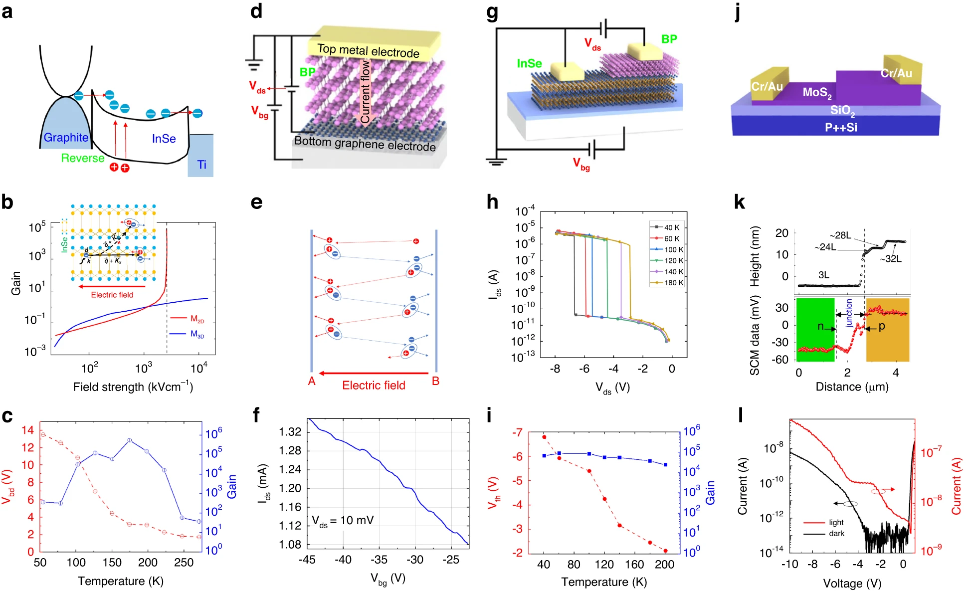
a graphite/InSe Schottky avalanche detector - injection, ionization, collection electron transport mechanisms, b e-ph scattering dimensionality reduction affects electron acceleration process and gain versus electric field in 2D (red line) and 3D (blue line), c breakdown voltage (Vbd) and gain as a function of temperature—exhibits a negative temperature coefficient81. Nanoscale vertical InSe/BP heterostructures ballistic avalanche photodetector: d schematic of the graphene/BP/metal avalanche device83, e ballistic avalanche photodetector operating principle, f quasi-periodic current oscillations, g schematic of the graphene InSe/BP83, h Ids–Vds characteristics for selected temperatures (40 − 180 K), i avalanche breakdown threshold voltage (Vth) and gain versus temperature—showing a negative temperature coefficient. Pristine PN junction avalanche photodetector: j device structure, k as the number of layers increases, a positive/negative signal of SCM denotes hole/electron carries, l APD’s low temperature (~100 K) dark and photocurrent I–V curves87
