Fig. 1
From: Isolated pairs of Majorana zero modes in a disordered superconducting lead monolayer

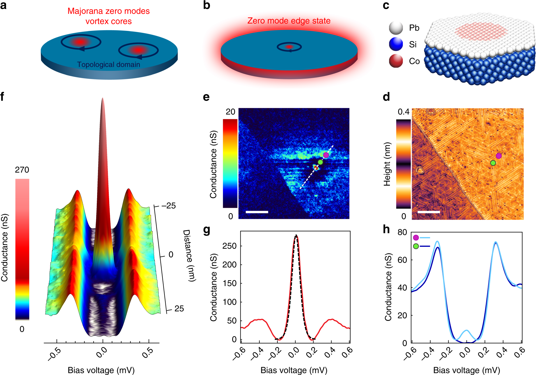
Spectroscopy of a pair of Majorana zero modes in atomic Pb monolayer. a Schematic view of a pair of vortices in a topological superconductor, each carrying a single Majorana zero mode. b Schematic view of a single vortex whose Majorana zero mode has to be paired with a Majorana zero mode surrounding the topological domain. c Schematic structure of the Pb/Co/Si(111) samples: a Co–Si magnetic domain is buried below a Pb monolayer. d Scanning tunneling microscopy image (scale bar is 20 nm) of the sample showing a Pb monolayer with devil’s staircase structure (VT = 50 mV, IT = 50 pA). The underlying Co–Si island doesnot appear in the topography. e Conductance map (scale bar is 20 nm) at VT = 0 mV showing a domain with a strong zero-bias peak dot (in red) surrounded by a gapped region (dark blue) itself surrounded by a zero-bias rim (light blue). f Conductance spectra along the linecut marked in e showing a very strong peak within the gap surrounded by a gapped area and another zero-bias peak (blue) outside of the domain. g Conductance curve taken at the center of the domain showing a very high zero-bias peak (Red curve). The dashed black curve is a fit with a state at E ≈ 6 μV with an electronic temperature of 350 mK. This can be considered as a zero-energy state within the precision of the experimental set-up. h The light blue conductance curve is taken on the domain rim (light blue in e) shows a peak at zero bias. The dark blue conductance curve is taken inside the dark blue region inside the domain, it shows a hard gap with no peak at zero bias. The green and purple markers in e and d indicate the position at which those spectrum were taken
