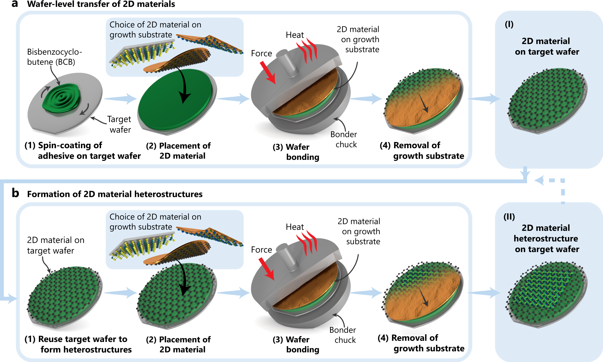
Fig. 1: Schematics illustration of the methodology for wafer-level transfer of two-dimensional (2D) materials and formation of 2D material heterostructures.
From: Large-area integration of two-dimensional materials and their heterostructures by wafer bonding

a Wafer-level transfer of materials. (1) Spin coating and soft baking of thermosetting bisbenzocyclobutene (BCB) as an adhesive layer on the target wafer. (2) Placement of the 2D material on its growth substrate on top of the target wafer, with the 2D material facing the target wafer. (3) Adhesive wafer bonding by applying heat and force to the wafer stack using a commercial semiconductor wafer bonding tool, thereby forming a stable bond between the 2D material on its growth substrate and the target wafer. (4) Removal of the growth substrate. (I) Transferred 2D material on the target wafer. b Formation of 2D material heterostructures. (1) Reusing the target wafer from step (I) without additional treatment. (2) Placement of a second 2D material on its growth substrate on top of the target wafer, with the 2D material facing the previously transferred 2D material. (3) Wafer bonding as in a) step (3). (4) Removing the growth substrate of the second 2D material. (II) Transferred 2D material heterostructure on the target wafer.
