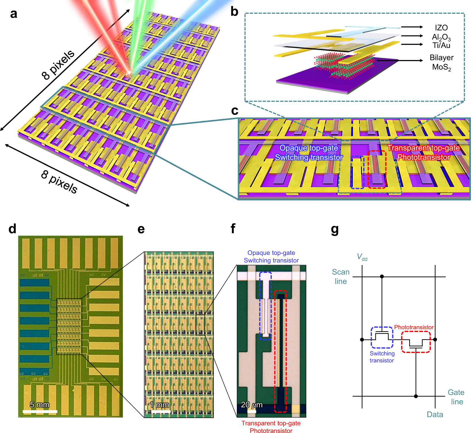
Fig. 1: Bilayer MoS2 image sensor array.

a Schematic illustration of an 8 × 8 image sensor array based on bilayer MoS2. b Cross-section of a pixel consisting of IZO, Al2O3, Ti/Au, and bilayer MoS2. c Image sensor array structure design composed of opaque top-gate (Ti/Au electrodes) switching transistor and transparent top-gate (IZO electrodes) phototransistor. d Low- and e high-magnification photograph of the 8 × 8 image sensor array based on bilayer MoS2. f Optical microscope image of a pixel composed of opaque top-gate switching transistor (blue-dashed line) and transparent top-gate phototransistor (red-dashed line). g A pixel circuit diagram of proposed image sensor array. Vdd is drain supply voltage.
