
Fig. 1: Exciting the correct acoustic mode of the wafer.
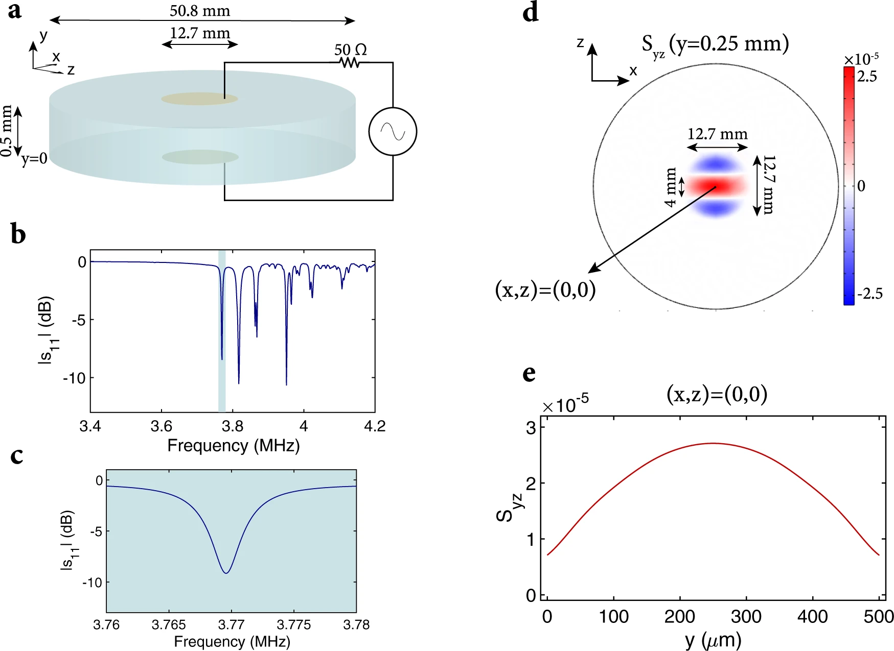
a A Y-cut lithium niobate wafer of diameter 50.8 mm and of thickness 0.5 mm is coated on top and bottom surfaces with electrodes having a diameter of 12.7 mm. The wafer is excited with an RF source through the top and bottom electrodes. b Simulated ∣s11∣ of the wafer with respect to 50 Ω, showing the resonances corresponding to different acoustic modes of the wafer (loss was added to lithium niobate to make it consistent with experimental results). The desired acoustic mode appears around 3.77 MHz and is highlighted in blue. c The desired acoustic mode ∣s11∣ with respect to 50 Ω is shown in more detail. d The dominant strain distribution (Syz) when the wafer is excited at 3.7696 MHz with 2 Vpp is shown for the center of the wafer. This strain distribution corresponds to the ∣s11∣ resonance shown in (c). e The variation in Syz parallel to the wafer normal and centered along the wafer is shown when the wafer is excited at 3.7696 MHz with 2 Vpp.
