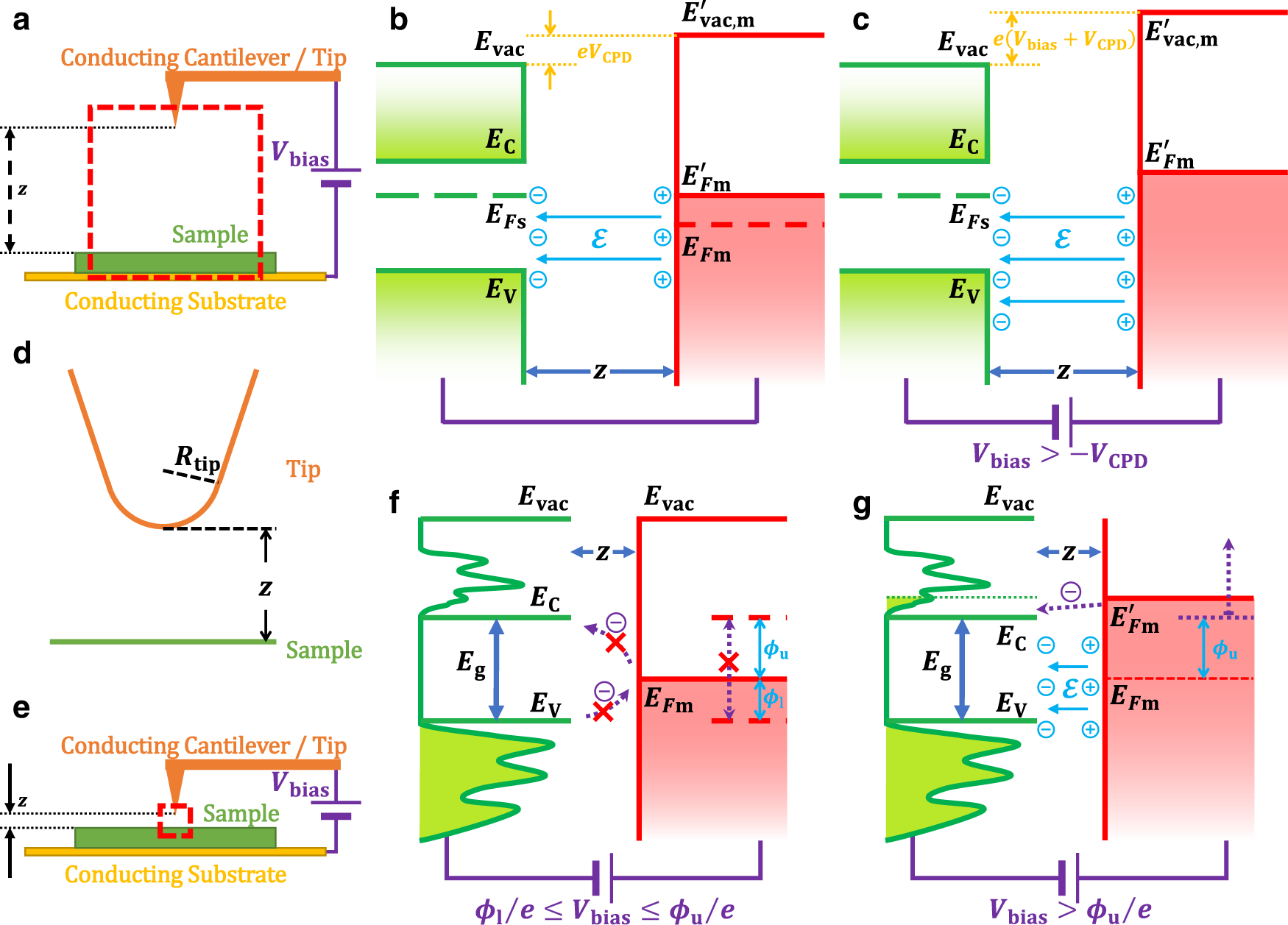
Fig. 1: Working principle of localized electric force microscopy (LEFM).

a The schematic diagram of the regular electric force microscopy (EFM). Here \({V}_{{{{{{\rm{bias}}}}}}}\) is the scanning external bias voltage and \(z\) is the tip-sample separation. b The energy level alignment between the conductive tip and the sample at the regular EFM without bias (\({V}_{{{{{{\rm{bias}}}}}}}=0\)). Here \({E}_{{{{{{\rm{vac}}}}}}}\), \({E}_{{{{{{\rm{C}}}}}}}\), \({E}_{F{{{{{\rm{s}}}}}}}\), and \({E}_{{{{{{\rm{V}}}}}}}\) denote the vacuum level, conduction band edge, Fermi level, and valance band edge of the sample, respectively. The charge transfer between the sample and tip aligns the Fermi level \({E}_{F{{{{{\rm{m}}}}}}}\) and consequently twists the Fermi level to \({E}_{F{{{{{\rm{m}}}}}}}^{{\prime} }\) and vacuum level to \({E}_{{{{{{\rm{vac}}}}}},{{{{{\rm{m}}}}}}}^{{\prime} }\) by the amount of contact potential difference \({V}_{{{{{{\rm{CPD}}}}}}}\), and builts up a local electric field \({{{{{\mathcal{E}}}}}}\) between the samples and the tip. c The energy alignment between the tip and the sample under an external bias at finite temperature in regular cases. d The capacitor model of the EFM system which consists of the conductive AFM tip with an apex curve of \({R}_{{{{{{\rm{tip}}}}}}}\) and the sample plane. e The schematic diagram of the LEFM model in which the EFM tip is pushed close to the sample and the local electric field is dominated by a nanoscale area. f When the external bias is not large enough to push the tip’s Fermi level out of the energy bandgap \({E}_{{{{{{\rm{g}}}}}}}\), charge transfer cannot take place and \({E}_{F{{{{{\rm{m}}}}}}}\) is pinned (purple arrows blocked by red crosses). Here \({\phi }_{{{{{{\rm{u}}}}}}}\)/\({\phi }_{{{{{{\rm{l}}}}}}}\) denotes the upper/lower energy difference between \({E}_{F{{{{{\rm{m}}}}}}}\) and \({E}_{{{{{{\rm{C}}}}}}}\)/\({E}_{{{{{{\rm{V}}}}}}}\). g When \({V}_{{{{{{\rm{bias}}}}}}}\) pushes \({E}_{F{{{{{\rm{m}}}}}}}\) in alignment with the conduction or valance band of the sample, the adequate density of states makes charge transfer possible (purple arrows) and electric field \({{{{{\mathcal{E}}}}}}\) is built up consequently.
