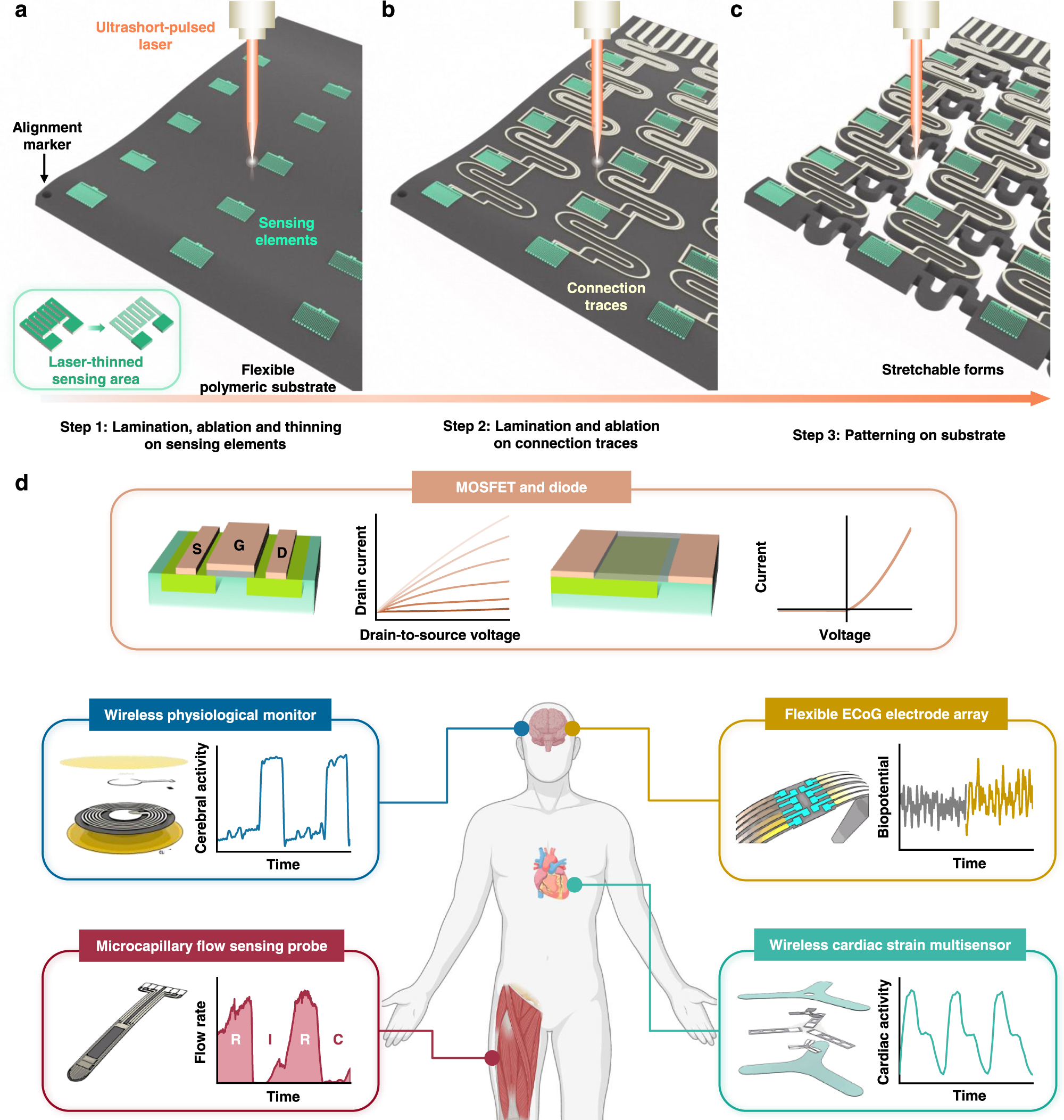
Fig. 1: Laser ablation processes for fabricating advanced multi-layered bioresorbable electronics.

Laser ablation fabrication procedures for bioresorbable electronics, including patterning of sensing elements and structuring of alignment markers (a), patterning of connection traces (b), and structuring substrates into stretchable forms (c). Inset: laser thinning process on the sensing elements in a. d Illustrations of a representative collection of bioresorbable electronic systems fabricated using these procedures, such as Si-based semiconductor devices and a series of sensors of pressure, cardiopulmonary activity, thermal transport, fluid flow, biopotential, and mechanical strain, for various organs and biomedical applications. System examples include wireless monitors for physiological parameters in tissue cavities, probes for microcapillary flow sensing in transplanted tissues/organs, flexible Si-based electrode arrays for biopotential recordings, and wireless systems for measuring principal and shear strains on the epicardial surface.
