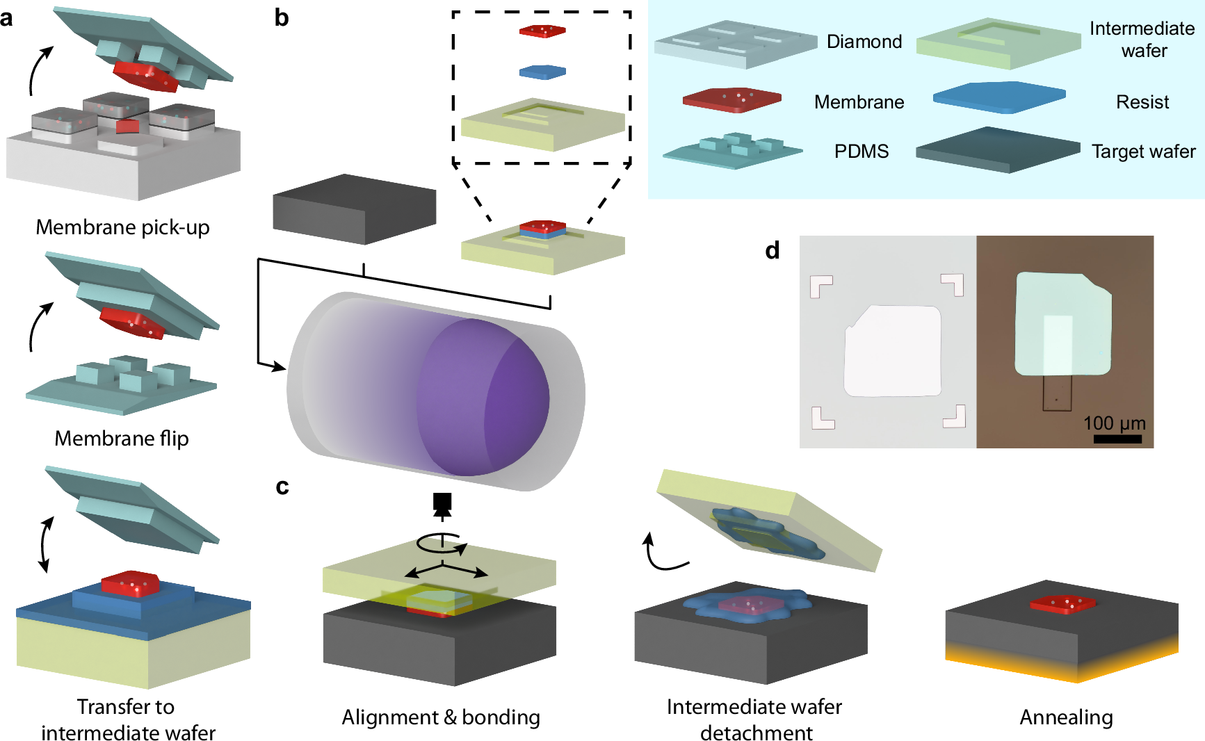
Fig. 1: Schematics of the plasma-activated bonding of diamond membranes.
From: Direct-bonded diamond membranes for heterogeneous quantum and electronic technologies

a Diamond membrane transfer to the intermediate wafer. From top to down: membrane pick-up from the diamond substrate using PDMS1-stamp, membrane flipping with PDMS2-stamp, membrane placement to a photoresist or electron beam resist covered intermediate wafer. b Diamond back etching and downstream oxygen plasma treatment. Inset: the detailed layer stack of the ICP-etched intermediate wafer. c Plasma-activated membrane bonding. Left to right: membrane alignment and bonding, temperature-controlled intermediate wafer detachment, and post-bonding annealing. d Microscope images of 155-nm-thick diamond membranes bonded to a thermal oxide substrate with markers (left) and a fused silica substrate with a 5-μm-deep trench etched prior to bonding (right).
