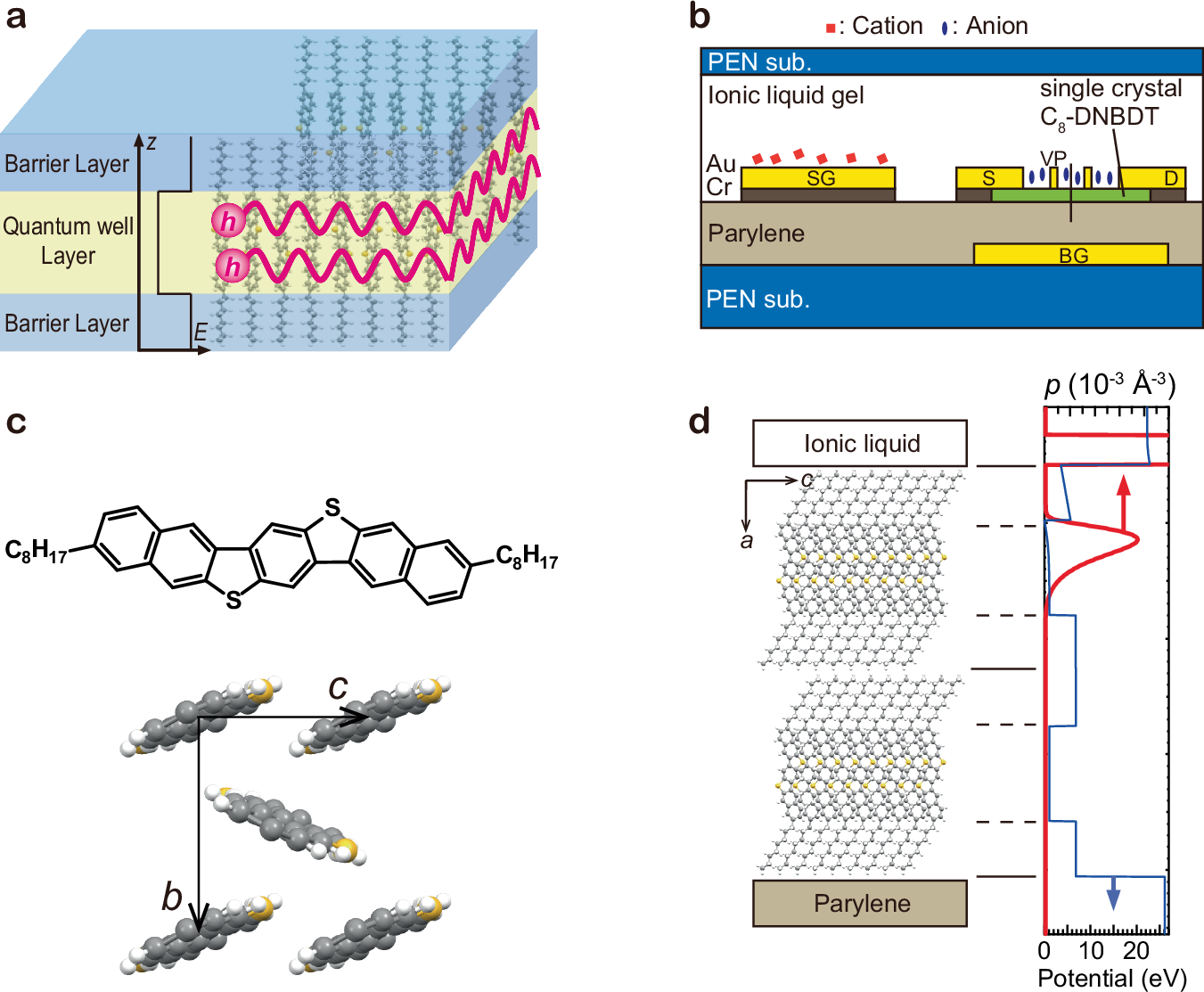
Fig. 1: Illustrations of electric-double-layer gated transistor using quantum-well molecules.
From: Evolution of electronic correlation in highly doped organic two-dimensional hole gas

a Schematic picture of a quantum-well molecular compound. b Schematic image of an electric-double-layer transistor. Here, S, D, BG, SG, and VP stand for the source, drain, bottom-gate, side-gate, and voltage probe, respectively. c Structural formula of a C8-DNBDT molecule (Upper) and the herringbone structure in the bc plane of the single crystal (Lower). Alkyl chains are omitted for visibility. d Cross section across ionic liquid/bilayer C8-DNBDT/parylene, and the hole distribution (red line, upper horizontal axis) and potential height (blue line) against the depth direction (vertical axis). The hole distribution is calculated by the Poisson–Schrödinger equation.
