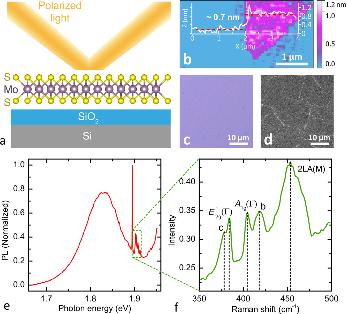
Fig. 1: Characterization of the monolayer sample.
From: Broadband optical properties of monolayer and bulk MoS2

a The scheme of the ellipsometry measurements. b AFM topography mapping and a cross-sectional profile of the edge of monolayer MoS2 on SiO2/Si substrate. The scan area was 4.5 × 2.1 μm.2 c Optical image of the MoS2 on top of SiO2/Si substrate. MoS2 covers more than 97% of the surface. d SEM image of the MoS2 revealing a high crystallinity of the samples with the crystallite size 8.4 ± 2.1 μm. e Photoluminescence of the monolayer MoS2 due to the recombination of the A-excitons. High photoluminescence response due to monolayer MoS2 being a direct gap semiconductor, unlike its bulk counterpart. f Resonant Raman spectrum of the MoS2 film at excitation wavelength λ = 632.8 nm. The Raman spectral features are labeled according to Chakraborty and et al.37. The positions of two first-order Raman modes, namely the \(E_{2{\mathrm{g}}}^1\) = 384 cm−1 and the \(A_{1g}\) = 404 cm−1, which are sensitive to the number of layers, correspond to a monolayer37.
