Abstract
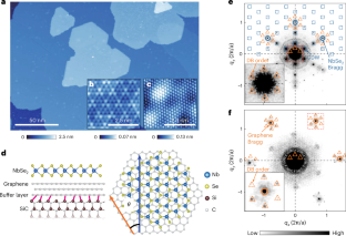
Superconductivity serves as a basis for non-trivial quantum phenomena and devices, but they often require artificial control of the superconducting gap. In real space, there are various ways to tailor the superconducting gap, such as by introducing interfaces and defects. However, it is challenging to manipulate the superconducting gap in momentum space. Here we demonstrate that the superconducting gap of NbSe2 monolayers on graphene can be modified at specific momenta by changing the twist angle between the layers. Our spectroscopic-imaging-based scanning tunnelling microscopy experiments reveal the interference patterns of Bogoliubov quasiparticles that are twisted with respect to NbSe2 and graphene lattices. We find that these chiral interference patterns originate from the twist-dependent sextet of regions in momentum space in which the Fermi surfaces of the NbSe2 monolayer and graphene overlap. This finding not only broadens our understanding of superconductivity in twisted bilayer systems but also opens up possibilities for designing artificial superconducting materials and devices with tunable properties.
This is a preview of subscription content, access via your institution
Access options
Access Nature and 54 other Nature Portfolio journals
Get Nature+, our best-value online-access subscription
$32.99 / 30 days
cancel any time
Subscribe to this journal
Receive 12 print issues and online access
$259.00 per year
only $21.58 per issue
Buy this article
- Purchase on SpringerLink
- Instant access to the full article PDF.
USD 39.95
Prices may be subject to local taxes which are calculated during checkout


Data availability
Additional data supporting the findings of this study are available from the corresponding authors upon reasonable request. Source data are provided with this paper.
Code availability
The codes supporting the findings of this study are available from the corresponding authors upon reasonable request.
References
Geim, A. K. & Grigorieva, I. V. Van der Waals heterostructures. Nature 499, 419–425 (2013).
Novoselov, K. S., Mishchenko, A., Carvalho, A. & Neto, A. H. C. 2D materials and van der Waals heterostructures. Science 353, aac9439 (2016).
Liu, Y., Huang, Y. & Duan, X. Van der Waals integration before and beyond two-dimensional materials. Nature 567, 323–333 (2019).
Novoselov, K. S. et al. Electric field effect in atomically thin carbon films. Science 306, 666–669 (2004).
Mak, K. F., Lee, C., Hone, J., Shan, J. & Heinz, T. F. Atomically thin MoS2: a new direct-gap semiconductor. Phys. Rev. Lett. 105, 136805 (2010).
Splendiani, A. et al. Emerging photoluminescence in monolayer MoS2. Nano Lett. 10, 1271–1275 (2010).
Deng, Y. et al. Gate-tunable room-temperature ferromagnetism in two-dimensional Fe3GeTe2. Nature 563, 94–99 (2018).
Seyler, K. L. et al. Ligand-field helical luminescence in a 2D ferromagnetic insulator. Nat. Phys. 14, 277–281 (2018).
Fu, L. & Kane, C. L. Superconducting proximity effect and Majorana fermions at the surface of a topological insulator. Phys. Rev. Lett. 100, 096407 (2008).
Xu, J.-P. et al. Artificial topological superconductor by the proximity effect. Phys. Rev. Lett. 112, 217001 (2014).
Xu, J.-P. et al. Experimental detection of a Majorana mode in the core of a magnetic vortex inside a topological insulator-superconductor Bi2Te3/NbSe2 heterostructure. Phys. Rev. Lett. 114, 017001 (2015).
Lüpke, F. et al. Proximity-induced superconducting gap in the quantum spin Hall edge state of monolayer WTe2. Nat. Phys. 16, 526–530 (2020).
Kezilebieke, S. et al. Moiré-enabled topological superconductivity. Nano Lett. 22, 328–333 (2022).
Bistritzer, R. & MacDonald, A. H. Moiré bands in twisted double-layer graphene. Proc. Natl Acad. Sci. USA 108, 12233–12237 (2011).
Kennes, D. M. et al. Moiré heterostructures as a condensed-matter quantum simulator. Nat. Phys. 17, 155–163 (2021).
Cao, Y. et al. Unconventional superconductivity in magic-angle graphene superlattices. Nature 556, 43–50 (2018).
Yankowitz, M. et al. Tuning superconductivity in twisted bilayer graphene. Science 363, 1059–1064 (2019).
Lu, X. et al. Superconductors, orbital magnets and correlated states in magic-angle bilayer graphene. Nature 574, 653–657 (2019).
Oh, M. et al. Evidence for unconventional superconductivity in twisted bilayer graphene. Nature 600, 240–245 (2021).
Wilson, J. A., Salvo, F. J. D. & Mahajan, S. Charge-density waves and superlattices in the metallic layered transition metal dichalcogenides. Adv. Phys. 50, 1171–1248 (2001).
Moncton, D. E., Axe, J. D. & DiSalvo, F. J. Study of superlattice formation in 2H-NbSe2 and 2H-TaSe2 by neutron scattering. Phys. Rev. Lett. 34, 734–737 (1975).
Revolinsky, E., Spiering, G. & Beerntsen, D. Superconductivity in the niobium-selenium system. J. Phys. Chem. Solids 26, 1029–1034 (1965).
Ugeda, M. M. et al. Characterization of collective ground states in single-layer NbSe2. Nat. Phys. 12, 92–97 (2016).
Xi, X. et al. Ising pairing in superconducting NbSe2 atomic layers. Nat. Phys. 12, 139–143 (2016).
Wang, H. et al. High-quality monolayer superconductor NbSe2 grown by chemical vapour deposition. Nat. Commun. 8, 394 (2017).
Xing, Y. et al. Ising superconductivity and quantum phase transition in macro-size monolayer NbSe2. Nano Lett. 17, 6802–6807 (2017).
Zhao, K. et al. Disorder-induced multifractal superconductivity in monolayer niobium dichalcogenides. Nat. Phys. 15, 904–910 (2019).
Chen, Y. et al. Visualizing the anomalous charge density wave states in graphene/NbSe2 heterostructures. Adv. Mater. 32, 2003746 (2020).
Dreher, P. et al. Proximity effects on the charge density wave order and superconductivity in single-layer NbSe2. ACS Nano 15, 19430–19438 (2021).
Ganguli, S. C., Vaňo, V., Kezilebieke, S., Lado, J. L. & Liljeroth, P. Confinement-engineered superconductor to correlated-insulator transition in a van der Waals monolayer. Nano Lett. 22, 1845–1850 (2022).
Zhang, Z., Watanabe, K., Taniguchi, T. & LeRoy, B. J. Local characterization and engineering of proximitized correlated states in graphene/Nbse2 vertical heterostructures. Phys. Rev. B 102, 085429 (2020).
Coletti, C. et al. Charge neutrality and band-gap tuning of epitaxial graphene on SiC by molecular doping. Phys. Rev. B 81, 235401 (2010).
Machida, T., Kohsaka, Y. & Hanaguri, T. A scanning tunneling microscope for spectroscopic imaging below 90 mK in magnetic fields up to 17.5 T. Rev. Sci. Instrum. 89, 093707 (2018).
Goler, S. et al. Revealing the atomic structure of the buffer layer between SiC(0001) and epitaxial graphene. Carbon 51, 249–254 (2013).
Riedl, C., Coletti, C. & Starke, U. Structural and electronic properties of epitaxial graphene on SiC(0001): a review of growth, characterization, transfer doping and hydrogen intercalation. J. Phys. D: Appl. Phys. 43, 374009 (2010).
Kohsaka, Y. et al. An intrinsic bond-centered electronic glass with unidirectional domains in underdoped cuprates. Science 315, 1380–1385 (2007).
Pham, T. T. et al. Higher-indexed moiré patterns and surface states of MoTe2/graphene heterostructure grown by molecular beam epitaxy. npj 2D Mater. Appl. 6, 48 (2022).
Liu, G.-B., Shan, W.-Y., Yao, Y., Yao, W. & Xiao, D. Three-band tight-binding model for monolayers of group-VIB transition metal dichalcogenides. Phys. Rev. B 88, 085433 (2013).
Arguello, C. J. et al. Quasiparticle interference, quasiparticle interactions, and the origin of the charge density wave in 2H-NbSe2. Phys. Rev. Lett. 114, 037001 (2015).
Gao, S. et al. Atomic-scale strain manipulation of a charge density wave. Proc. Natl Acad. Sci. USA 115, 6986–6990 (2018).
Liu, X., Chong, Y. X., Sharma, R. & Davis, J. C. S. Discovery of a Cooper-pair density wave state in a transition-metal dichalcogenide. Science 372, 1447–1452 (2021).
Cao, L. et al. Directly visualizing nematic superconductivity driven by the pair density wave in NbSe2. Nat. Commun. 15, 7234 (2024).
Brun, C. et al. Dynamical Coulomb blockade observed in nanosized electrical contacts. Phys. Rev. Lett. 108, 126802 (2012).
Devoret, M. H. et al. Effect of the electromagnetic environment on the Coulomb blockade in ultrasmall tunnel junctions. Phys. Rev. Lett. 64, 1824–1827 (1990).
Ingold, G.-L. & Nazarov, Y. V. Charge Tunneling Rates in Ultrasmall Junctions 21–107 (Springer, 1992).
Ast, C. R. et al. Sensing the quantum limit in scanning tunnelling spectroscopy. Nat. Commun. 7, 13009 (2016).
Gor’kov, L. P. & Rashba, E. I. Superconducting 2D system with lifted spin degeneracy: mixed singlet-triplet state. Phys. Rev. Lett. 87, 037004 (2001).
Gani, Y. S., Steinberg, H. & Rossi, E. Superconductivity in twisted graphene NbSe2 heterostructures. Phys. Rev. B 99, 235404 (2019).
Li, Y. & Koshino, M. Twist-angle dependence of the proximity spin-orbit coupling in graphene on transition-metal dichalcogenides. Phys. Rev. B 99, 075438 (2019).
Asano, S. & Yanase, Y. Tuning monolayer superconductivity in twisted NbSe2 graphene heterostructures. Phys. Rev. B 110, 134516 (2024).
Sticlet, D. & Morari, C. Topological superconductivity from magnetic impurities on monolayer NbSe2. Phys. Rev. B 100, 075420 (2019).
Acknowledgements
We thank C. J. Butler, M. Nakano, K. Sugawara, Y. Okada, Y. Hasegawa and P. Wahl for valuable discussions and comments. This work was supported by the RIKEN TRIP initiative (Many-Body Electron Systems) and JSPS KAKENHI grant nos. JP19H05824, JP21K18145, JP22H04933, JP22K18696, JP22K20362, JP23K13067, JP23K17353, JP23K22452, JP23K25831 JP24H00007, JP24K21530 and JST PRESTO JPMJPR19L8. M.N. acknowledges support from RIKEN’s SPDR fellowship.
Author information
Authors and Affiliations
Contributions
M.N. prepared the samples, carried out the SI-STM measurements and analysed the data with assistance from T.M. S.A. and Y.Y. contributed to the construction of the sextet model. T.H. supervised the project. M.N. and T.H. wrote the manuscript. All authors discussed the results and contributed to finalizing the manuscript.
Corresponding authors
Ethics declarations
Competing interests
The authors declare no competing interests.
Peer review
Peer review information
Nature Physics thanks Somesh Ganguli and the other, anonymous, reviewer(s) for their contribution to the peer review of this work.
Additional information
Publisher’s note Springer Nature remains neutral with regard to jurisdictional claims in published maps and institutional affiliations.
Supplementary information
Supplementary Information
Supplementary Figs. 1–7 and Notes 1–5.
Rights and permissions
Springer Nature or its licensor (e.g. a society or other partner) holds exclusive rights to this article under a publishing agreement with the author(s) or other rightsholder(s); author self-archiving of the accepted manuscript version of this article is solely governed by the terms of such publishing agreement and applicable law.
About this article
Cite this article
Naritsuka, M., Machida, T., Asano, S. et al. Superconductivity controlled by twist angle in monolayer NbSe2 on graphene. Nat. Phys. 21, 746–753 (2025). https://doi.org/10.1038/s41567-025-02828-6
Received:
Accepted:
Published:
Version of record:
Issue date:
DOI: https://doi.org/10.1038/s41567-025-02828-6
This article is cited by
-
Phase engineering of relaxor ferroelectricity in van der Waals crystal
Nature Communications (2026)


