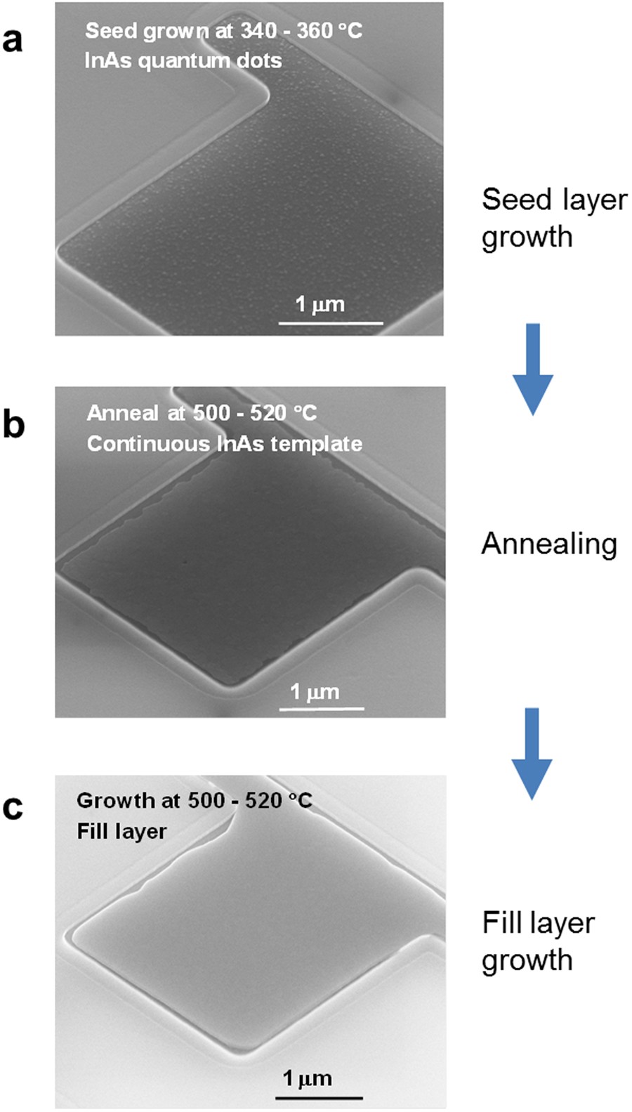
Figure 1

SEM images of InAs epitaxial layers directly grown on Si(111) showing stages in the epitaxial growth process. (a) The InAs seed grown at 340–360 °C shows many InAs quantum dots about 20–30 nm in diameter. (b) Annealing at 500–520 °C causes the dots to merge into a single two-dimensional InAs template layer. (c) Fill layer growth provides a layer of target thickness.
