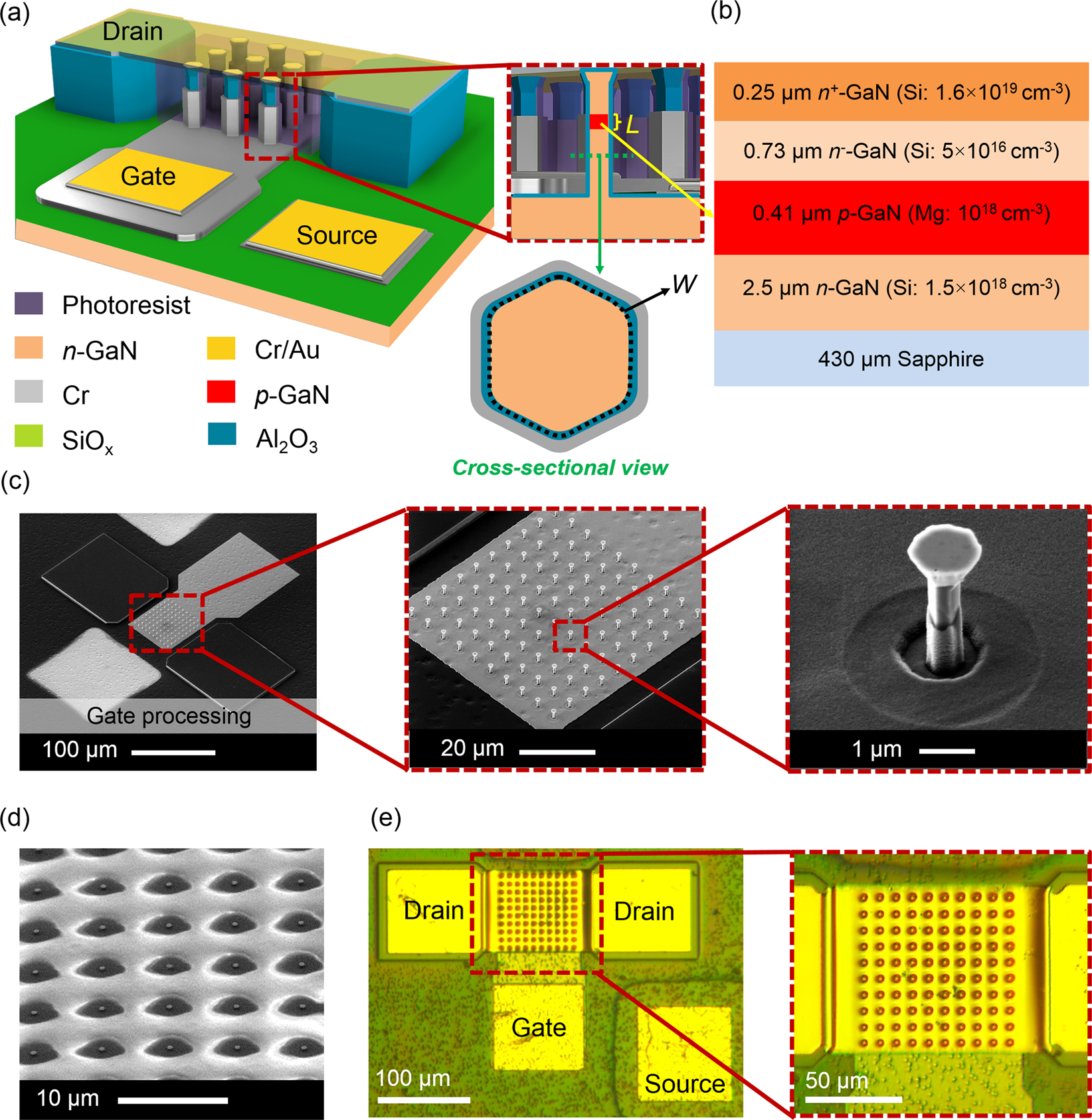
Figure 1
From: Top-down GaN nanowire transistors with nearly zero gate hysteresis for parallel vertical electronics

(a) 3D schematics of a 9 n-p-n vertical GaN NW FET with L and W as gate length and gate width in inset, respectively, and (b) wafer composition used in this work. Fabrication process steps for creating 1, 9, and 100 NW FETs after (c) Cr gate processing, (d) photoresist filling, short UV exposure, and curing for 30 min at 250 °C, (e) e-beam evaporation of Cr/Au (80/200 nm) and subsequent etch-back process to form metal drain contact on n-p-n vertical GaN NW array.
