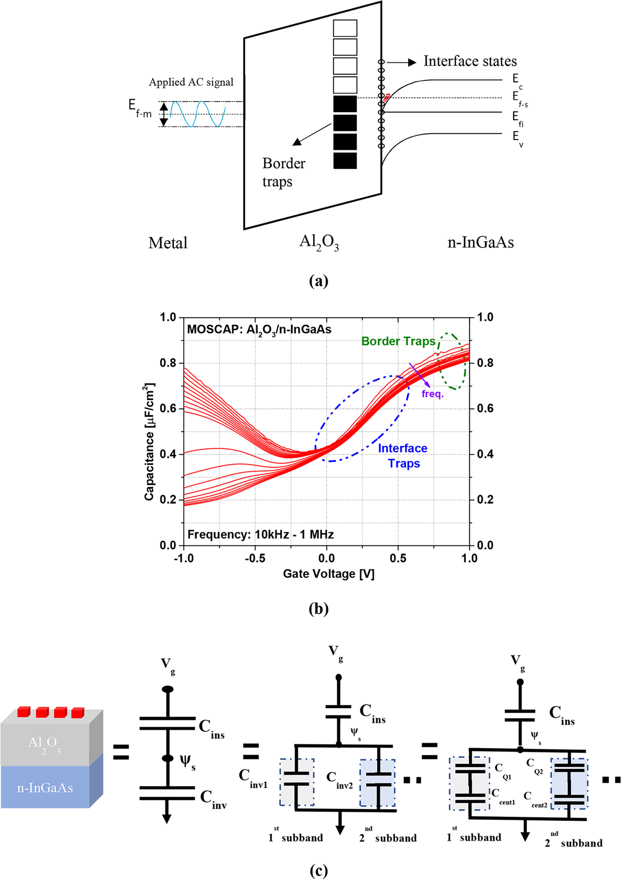
Figure 1

(a) Energy-band diagram of a metal/Al2O3/n-InGaAs MOS capacitor with the interface and border traps when an AC signal is applied. (b) Response regions of the interface and border traps in the capacitance-voltage (C-V) behavior of the Al2O3/n-InGaAs MOS capacitor. (c) Equivalent circuit diagram for the gate capacitance of the III–V MOSFET.
