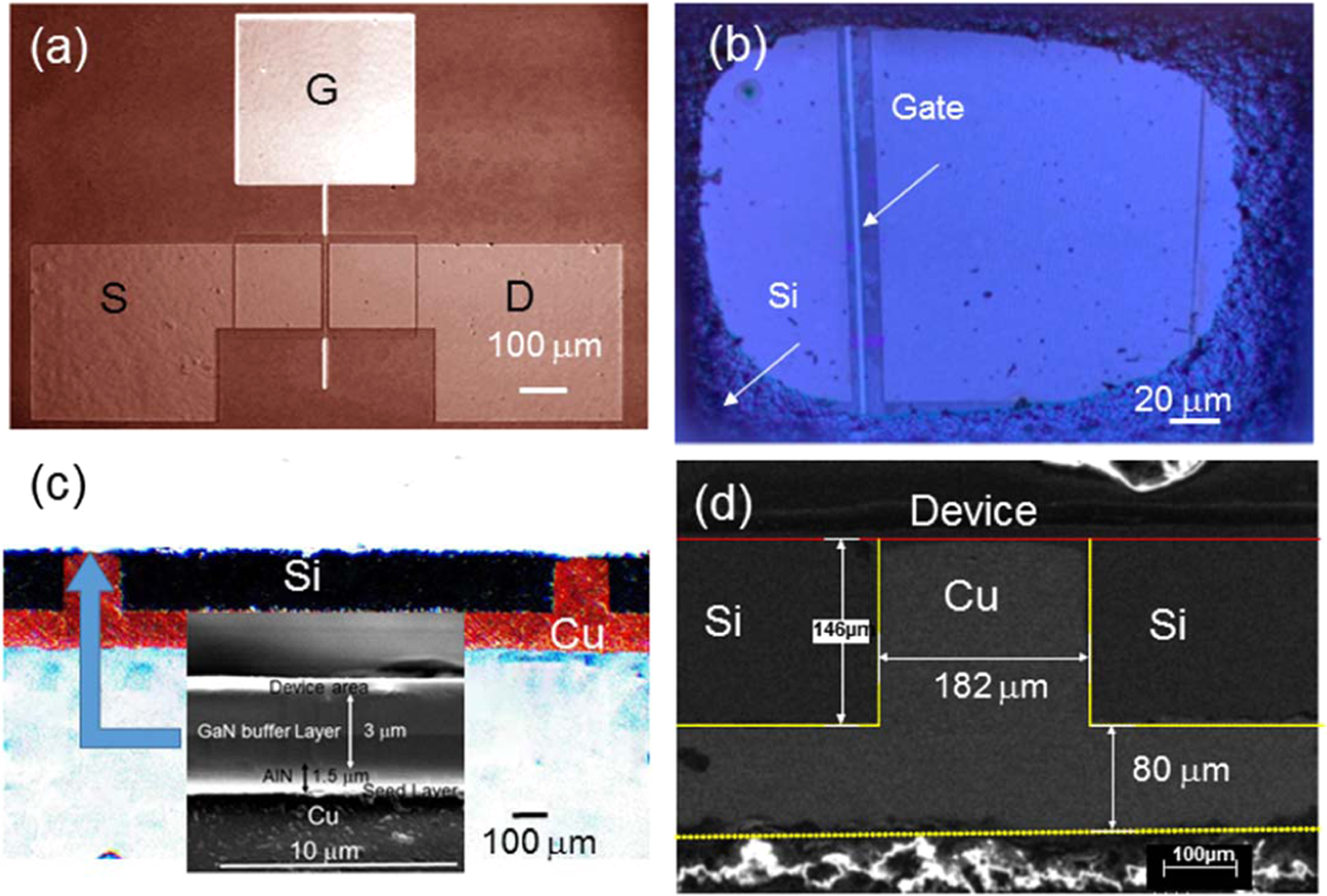
Figure 1

(a) OM top view of fabricated GaN HEMT on silicon, (b) OM backside view of the HEMT structure after complete removal of the Si, (c) OM cross-section view of the copper filled trench structure, and (d) SEM cross-sectional view after copper filling in the micro-trench region. The inset of (c) is the device structure above the Cu.
