Figure 1
From: A highly stable, nanotube-enhanced, CMOS-MEMS thermal emitter for mid-IR gas sensing

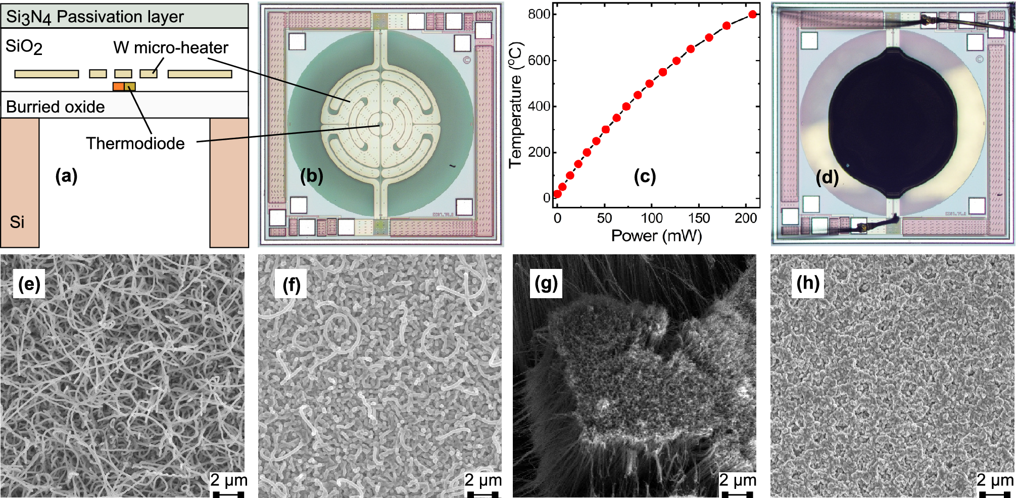
Device fabrication. (a) Micro-hotplate cross-section (not to scale) employing a tungsten (W) heating element embedded into a \(\sim\) 5 \(\upmu\)m thick silicon dioxide (SiO\(_2\)) membrane formed by deep reactive ion etching. (b) Optical image of the micro-hotplate, showing a multi-ring designed heating element surrounded by the membrane. Chip size = 1.76 mm \(\times\) 1.76 mm. (c) Micro-heater temperature as a function of power consumption. (d) The active heating element serves three purposes: (i) localised in-situ heating (micro-reactor) during the CNT growth process; (ii) employed as thermal profiler (adlayer flashing) for self-annealing; and (iii) used to generate IR emission during device operation (typically at temperatures of 300–600 \(^{\circ }\)C). (e) Typical SEM image of spaghetti-like CNT structure grown by an in-situ CVD process using acetylene (C\(_2\)H\(_2\)) blended with ammonia (NH\(_3\)) over an iron (Fe) catalyst, and (f) their SEM image after \(\sim\) 50 nm alumina (Al\(_2\)O\(_3\)) encapsulation. (e) SEM image of denser, more aligned CNTs synthesised by mixing C\(_2\)H\(_2\) with hydrogen (H\(_2\)), and (h) their SEM image after encapsulation.
