Figure 1
From: Impact of device scaling on the electrical properties of MoS2 field-effect transistors

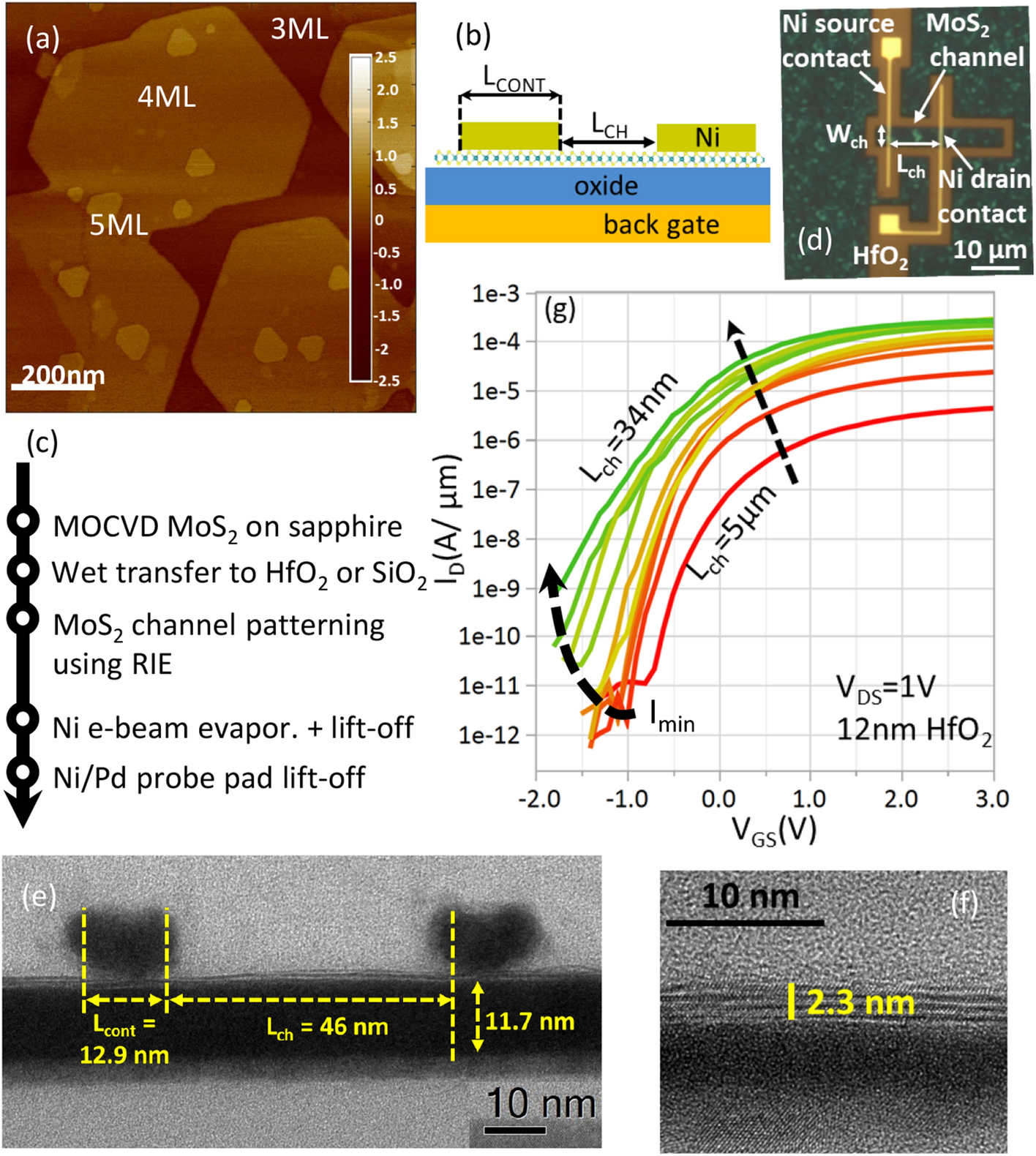
(a) Atomic force micrograph of CVD MoS2 on sapphire template shows a closed 3ML layer with islands of 4 and 5 monolayers distributed randomly. (b) Device schematic with global back-gate and top source/drain contacts. (c) Fabrication flow for the back-gated devices. (d) Optical micrograph showing the patterned MoS2 channel with 10 nm thick Ni contacts. (e) Cross-TEM shows a fabricated device with Lcont = 13 nm and Lch = 46 nm on 12 nm HfO2. (f) Zoom-in of the channel region for another device showing 3 monolayer MoS2 on nominal 4 nm HfO2 (g) Transfer characteristics at a fixed VDS = 1 V. Maximum drive current at VGS = 3 V scales with Lch saturating for short-channel devices. The plot shows Lch = 34 nm, 44 nm, 50 nm, 70 nm, 100 nm, 200 nm, 300 nm, 500 nm, 1000 nm, 5000 nm.
