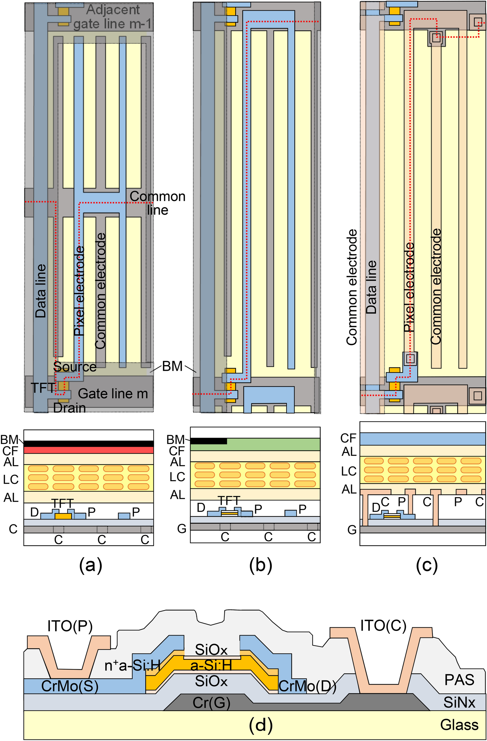
Figure 1

Pixel plane (top) and sectional views (bottom) of (a) the conventional structure, (b) the proposed CL structure without common line, (c) the proposed CLSE structure without common line and black matrix, with pixel and common electrodes made on the top of TFT substrate (G: gate, C: common, D: drain, P: pixel, AL: alignment layer, LC: liquid crystal, BM: black matrix, CF: color filter). Common electrodes are connected to the common line in the conventional structure, while they are connected to the adjacent gate line in the proposed structures. The red dotted line in each plane view indicates the cutting route for the corresponding sectional structure. (d) Detailed sectional structure of the CLSE structure.
