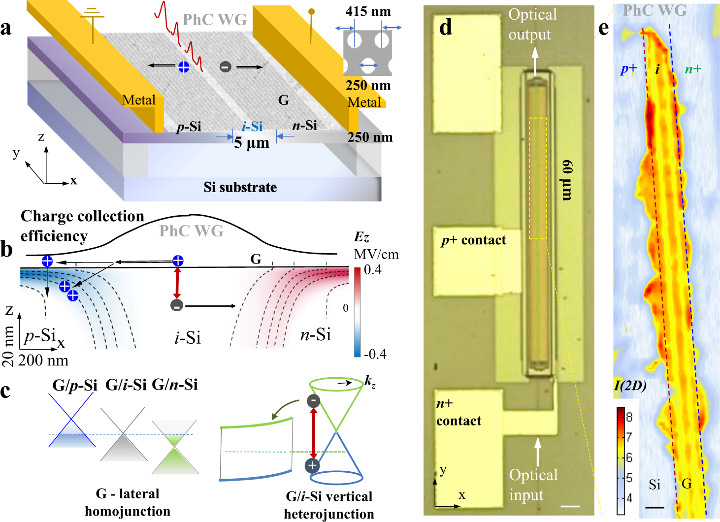
Fig. 1
From: Spatially controlled electrostatic doping in graphene p-i-n junction for hybrid silicon photodiode

Efficient carrier separation in Van der Waals contacted graphene-silicon p-i-n junction. a A schematic diagram to show the graphene-CMOS photonic crystal waveguide integration. The metal electrodes contact to the p and n sides of silicon membrane through Graphene, contacting onto the silicon photonic crystal membrane, is electrically isolated from the metal electrodes. Inset: lattice constant and hole diameter of photonic crystal design. b Vertical electric field near the graphene-silicon interface. Arrows indicate the moving direction of carriers driven by the built-in electric field. The charge collection efficiency peaks around the center of the graphene layer. c The quasi fermi level of the lateral homojunction and the optical absorption mechanism for photon energy in the infrared range, with charge carrier collection by Schottky barriers. d Top view of the device. Scale bar: 20 µm. e Raman 2D peak mapping of isolated piece of single layer graphene on the intrinsic part of suspended silicon p-i-n junction. The two bars in the middle part reflects the substrate waveguides design. Scale bar: 3 µm
