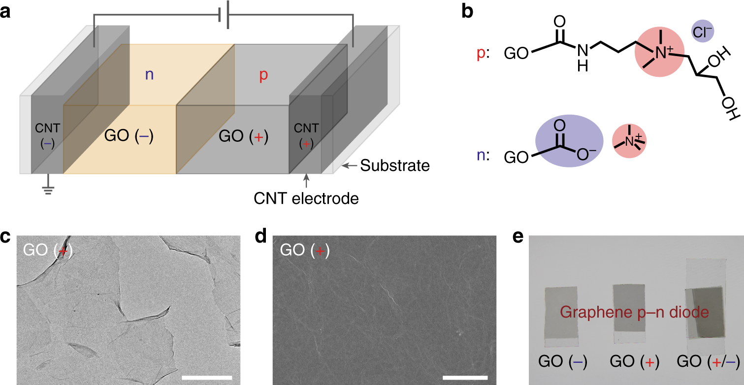
Fig. 1

Fabrication of an all carbon materials pn diode. a The scheme of an all carbon materials pn diode consisting of a 40 nm-thick negatively charged GO(−) layer (n), a 40 nm-thick positively charged GO(+) layer (p), two 20 nm-thick CNT conducive electrodes, and two transparent glass supports. b The molecular structures of chemically functionalized positively (p) and negatively (n) charged graphene oxides. The mobile counterions are chloride anion and tetramethyl ammonium cations, respectively. c The typical TEM image of highly dispersed positively charged GO sheets. Scale bar, 500 nm. d The surface morphology (SEM image) of a 40 nm-thick positively charged GO(+) layer with a 20 nm-thick CNT layer at the bottom. Scale bar, 2 μm. e The photographs of negatively charged GO layer (left, 40 nm-thick), positively charged GO layer (middle, 40 nm-thick), and laminated layers (right). (Note: both positively and negatively charged GO have conductive CNT electrodes (20 nm-thick) at the bottom)
