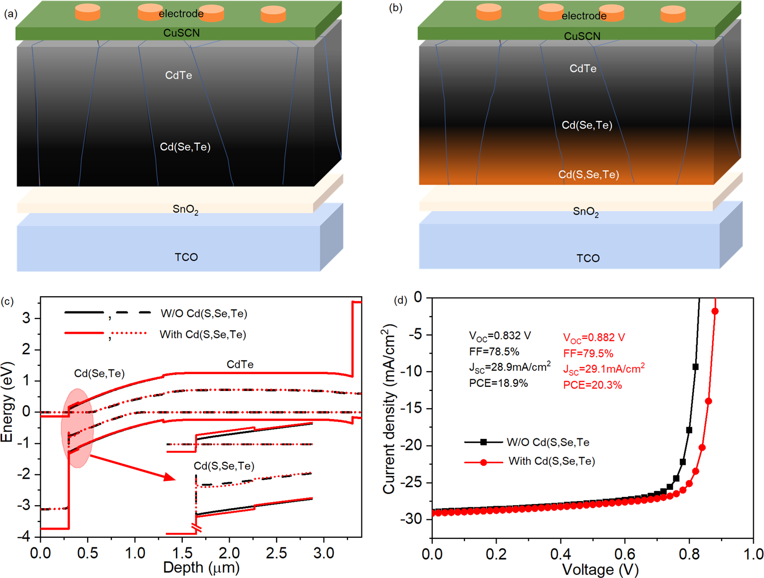
Fig. 1: Benefits of the bandgap gradient at the front junction.

Configurations of devices (a) without and (b) with a proposed bandgap gradient on the commercial SnO2 buffer layer and (c) the corresponding band alignment of the proposed devices. The solid black and red lines are almost completely overlapped because of the small change of bandgap caused by the Cd(S,Se,Te) region. The inset is used to present the difference in the band alignment at the Cd(S,Se,Te) region. d SCAPS simulated J–V curves for devices without and with the bandgap gradient at the front interface.
