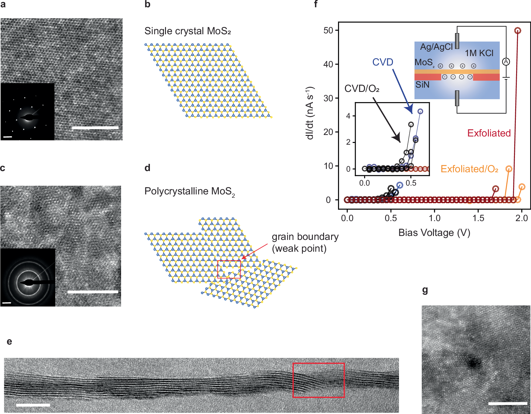
Fig. 1: Electrochemical pore creation in polycrystalline, few-layer MoS2 as compared to mechanically exfoliated few-layer single crystals.
From: In situ generation of (sub) nanometer pores in MoS2 membranes for ion-selective transport

STEM images and cartoons of few-layer single crystal ME-MoS2 (a, b) and polycrystalline CVD-MoS2 (c, d) with diffraction patterns inset. Continuous rings evident in the CVD-MoS2 diffraction pattern indicate that the grains are randomly rotated in-plane with respect to each other, and Moiré patterns evident in real-space images indicate that grains are partially overlapping. e Cross-section TEM image of polycrystalline MoS2, with a grain-boundary marked in red. f Change in ionic current for a given (constant) bias voltage applied across the membrane. A rapid, but controllable, increase in current is apparent for CVD-MoS2 at 0.4–0.5 V (inset), whereas a significantly more rapid, and difficult-to-control breakdown occurs for ME-MoS2 at 1.75-2 V. Partial oxidation of the film does not have a significant effect on the breakdown voltage. Device schematic is inset, showing ion accumulation leading to large electric fields across the membrane. g Polycrystalline MoS2, after electrochemical etching, showing a single (out of many) ~1 nm diameter pore. Scale bars are 5 nm in a, c and g; 2 nm-1 in (a) and (c) inset; and 10 nm in e. Source data for (f) are provided as a Source Data file.
