
Abstract
Efficient machine learning inference is essential for the rapid adoption of artificial intelligence (AI) across various domains. On-chip optical computing has emerged as a transformative solution due to its ultra-low power consumption, yet improving computational density remains challenging because of the difficulty of miniaturizing interference-based components. Here, we demonstrate fabrication-constrained scattering optical computing within nanophotonic media, enabled by fabrication-aware inverse design. This yields an ultra-compact optical neural architecture occupying 64 µm²—a three-order reduction compared to conventional optical neural networks. Our prototype achieves 86.7% accuracy on the Iris dataset, closely matching simulations. To further validate scalability, we train a larger 64-input design for optical character recognition using 8×8 handwritten digits, reaching 92.8% test accuracy. These results highlight the potential of nanophotonic media to perform large-scale tasks in ultra-small footprints, paving the way for dense, energy-efficient optical processors for next-generation AI.
Introduction
Large-scale machine learning models are driving transformative advances across various industries, with examples like generative pre-trained transformers revolutionizing natural language processing1 and vision transformers enhancing weather forecasting2. However, these breakthroughs come with a significant cost: a substantial increase in computational power demands. Traditional electronic computing platforms are reaching their limits in power efficiency, as further reductions in transistor energy consumption yield diminishing returns. As a result, integrated optical computing platforms, which offer reduced power consumption and inherent parallelism, are garnering increasing research attention3.
Integrated optical architectures for machine learning, such as Mach–Zehnder interferometer (MZI) meshes4,5, waveguide attenuators6,7, micro-rings8, and diffractive elements9,10,11,12,13, have been extensively explored as power-efficient solutions for optical neural computing. However, these architectures rely on systematically arranged units for phase and attenuation tuning, which are constrained by the empirical design principles of their constituent components, thus limiting further miniaturization. Recently, machine learning using nanophotonic media has emerged as a promising approach to reducing on-chip optical computation footprints by leveraging first-principles design14,15, with similar approaches also applied to on-chip matrix operations16,17. Nevertheless, the construction of compact and functional neural computing structures using nanophotonic media that seamlessly integrate fabrication constraints into the training process remains an experimental challenge. Developing such structures compatible with general fabrication technologies is eagerly pursued, as it holds the potential to unlock the full capabilities of integrated photonic platforms for machine learning applications.
In this work, we present an approach to on-chip optical computing, leveraging nanophotonic media to address the challenges of computational density and power efficiency in machine learning inference. We report the fabrication and experimental validation of neural computing structures on a silicon-on-insulator (SOI) platform using nanophotonic media, tested with the Iris flower dataset18. The design demonstrates a compact footprint of 64 µm2, which is several orders of magnitude smaller than typical on-chip optical neural networks that generally occupy areas on the scale of square millimeters. After training, the model achieved a test accuracy of 86.7%, with the experimental accuracy of the fabricated chip also reaching 86.7%. To achieve this, we developed a training method that incorporates fabrication constraints directly into the training process, coupled with low-index-contrast structures for enhancing fabrication tolerance. These innovations not only significantly reduce the device footprint but also offer scalability to more complex machine learning tasks. To further demonstrate the scalability of our approach, we applied it to a more complex dataset for handwritten digit image recognition, achieving a test accuracy of 92.8%. This work paves the way for ultra-compact, power-efficient optical neural computing systems, reducing the inference costs of large-scale machine learning models and providing a clear path toward scalable optical AI hardware.
Results
On-chip nanophotonic media configuration
On-chip optical devices can be conceptualized as systems that perform operations on a set of basic optical modes19. Similarly, on-chip analog computing systems process input information encoded in these basic modes and transform it into output modes carrying the desired information. The efficiency of this transformation, commonly referred to as coupling efficiency, directly determines the computational density of the on-chip optical computing system. As illustrated in Fig. 1a, coupling efficiency (κ), as predicted by coupled mode theory20, is influenced by refractive index perturbations within the system. Specifically, larger perturbations and greater refractive index contrasts result in higher coupling efficiencies. Consequently, enhancing these two factors is key to improving computational density in on-chip optical computing systems.
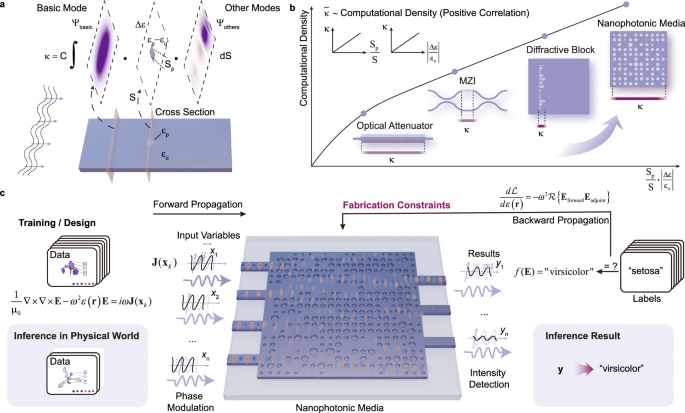
a Qualitative analysis for the coupling efficiency, which is related to the computational density in on-chip optical systems. b Comparison of different kinds of on-chip optical computational systems with computation-related coupling efficiency. c Schematic of the training and inference process of the nanophotonic media, where gradient information is calculated via the adjoint method and used to update the structures according to fabrication constraints. After fabrication, inference is achieved by light passing through the scattering nanophotonic media. Input information is encoded in the phase-modulated input light, and results are obtained through intensity detection at the output ports.
Figure 1b compares existing structures for on-chip optical computing systems with the proposed nanophotonic media, demonstrating that nanophotonic media can achieve relatively higher average efficiency. Traditional approaches, such as electrical tuning of doped waveguides, thermal tuning of waveguides, or etching diffractive structures, rely on explicit design theories. However, these methods are often constrained by empirical design principles, which limit their ability to achieve high mode coupling efficiency. In contrast, nanophotonic media enable high coupling efficiency within a compact area by overcoming the limitations of empirical design principles, thereby achieving greater computational density in on-chip systems. Nonetheless, the high coupling efficiency of nanophotonic media in such small regions also amplifies the sensitivity to fabrication-induced perturbations, which can introduce significant errors. Therefore, incorporating fabrication constraints into the design process of nanophotonic media is essential to ensure reliable system performance.
Machine learning inference in our approach is achieved using high computational density nanophotonic media, as shown in Fig. 1c, where the Iris flower classification task is taken as an example. Features are encoded into the phase modulation of waveguide eigenmodes on the left, while inference results are carried by the optical power in different output waveguides. The inference function is carried out by the nanophotonic media within the central block, where the radii of the holes in the nanophotonic media act as trainable parameters during the training process.
The training process can be viewed as solving an optimization problem under fabrication constraints and physical constraints:
where \({\mathcal L}\) is the loss function of the training process, and \({{\bf{T}}}=(\begin{array}{cccc}{{{\bf{E}}}}_{1} & {{{\bf{E}}}}_{2} & \ldots & {{{\bf{E}}}}_{n}\end{array})\) is a tensor that contains all the electric field responses with samples in the training dataset. \({{\bf{r}}}\) is the parameter to be optimized, which represents the radii of the holes in the nanophotonic media to be designed. \({{\bf{X}}}\) and \({{\bf{t}}}\) are features and labels of the training dataset. \(g\) is a function to apply fabrication constraints for each radius, and it is dynamically changed with respect to the nanophotonic media distribution. The second constraint is the physical constraint from the Maxwell Equations for the integrated optical structures with silicon and silica, where \({{{\rm{\mu }}}}_{0}\) is the permeability of vacuum, \({{\bf{E}}}\) is the electric field with the dielectric constant \(\varepsilon ({{\bf{r}}})\) and the optical source distribution \({{\bf{J}}}({{{\bf{x}}}}_{k})\) at an angular frequency of \(\omega\). The optical source distribution \({{\bf{J}}}({{{\bf{x}}}}_{k})\) is related to \({{{\bf{x}}}}_{k}\), which is the feature of a single sample in the training dataset.
We designed a gradient descent method with projection operations to solve this optimization problem. A schematic of the training process is shown in Fig. 2a. For each training sample, input sources on the left waveguides are reconfigured for simulation, and the resulting power intensities in the right waveguides are monitored and used to calculate the loss via a loss function. Gradients of the loss function with respect to the hole radii are then computed using the backpropagation method. The nanophotonic media are subsequently updated based on the gradient information and projection operations, incorporating fabrication constraints.

a Design flow of the structure parameters of the nanophotonic media with the features and label in the training dataset. b Structure parameters updating rules in each iteration. c Prediction accuracy and loss over 100 training iterations. d Confusion matrix on the test dataset. e–g The absolute value of the Poynting vector in x-direction for randomly selected inputs: e prediction of setosa; f prediction of versicolor; g prediction of virginica. h, i Comparison of designs with h no fabrication constraints and i fabrication constraints incorporated into the design process. j Comparison of the simulated fabrication variation under different fabrication tolerances with shallow etching and full etching, where vertical lines represent the 95% confidence interval.
Designing functional structures by solving optimization problems is classified as inverse design problems in integrated photonics, where ensuring the feasibility of fabricating the designed structures presents a significant challenge. An intuitive approach for ensuring fabricability involves selecting a design space that exclusively accommodates discrete, manufacturable geometries. Algorithms, such as the direct binary search (DBS) algorithm21, can be employed to explore this limited discrete design space. While this method consistently produces reliable results, it may restrict the degrees of freedom available for potential designs. Another approach for ensuring fabricability involves selecting a larger, continuous design space that includes non-fabricable geometries. Constraints are then applied within the algorithms to guide the inverse-designed structures away from these non-manufacturable geometries. Techniques like topology optimization22, shape optimization23, and methods integrated with the level-set method24 are successful and elegant for navigating continuous design spaces. In topology optimization, projection methods25 and morphological operations26 are commonly used to address non-manufacturability issues. By translating fabrication constraints into penalty terms within the optimization objectives, some methods integrated with the level-set approach have been developed to limit the minimum feature size and minimum radius of curvature27,28. Nonetheless, due to the non-convexity of inverse design problems and the discrete nature of the manufacturable design space, incorporating efficient fabrication constraints into inverse design methods remains a significant challenge.
In our approach, the design space is discretized into nano-block arrays while maintaining the radius of the hole structures within each block as continuously tunable, thereby achieving a large design parameter space. At the same time, we specify dynamically changing constraint rules to ensure that all hole structures meet fabrication constraints. After calculating the gradient information using the adjoint method23 in each iteration, we apply a projection operation based on the gradient information and the current structural state to optimize all structures under fabrication constraints until the iteration limit is reached (details and comparison with the topology optimization are described in Supplementary Note 1), as shown in Fig. 2b. The gradient information is obtained using samples and labels from the task dataset, enabling a training process for the structure to learn and adapt to the target task.
We use the Iris flower dataset to train and test the nanophotonic media. This dataset consists of 150 data points18 for classifying three types of Iris flowers: setosa, versicolor, and virginica. Each of the data points has four flower features. These features are normalized and rescaled to fit within the 0-π phase range of the eigenmode sources of the input waveguides. The nanophotonic media system is trained using 80% of the dataset, with the remaining 20% reserved for testing the trained system. The nanophotonic media that works as an Iris flower classification inference function is an 8×8 µm2 region in the center with 20 × 20 70 nm shallow etched holes, which is shown in Fig. 1c. Diameters of these holes vary from 130 to 400 nm, ensuring the fabricability. As part of the SOI platform, the 220 nm thick silicon material is on top of a 2 µm silicon oxide box and covered by 1 µm silicon oxide. Diameters of the holes are learned from the Iris flower dataset. After fabrication, the nanophotonic media can identify the category of an Iris flower with unlearned features.
A normalized mean square error (NMSE) loss function (details in Supplementary Note 2) and a batch gradient descent strategy using the adaptive moment estimation (Adam) optimization algorithm are employed for the training process. Figure 2c and Fig. 2d illustrate the evolution of the NMSE loss, prediction accuracy in the training process, and the confusion matrix on the test dataset after training, respectively. An accuracy of 86.7% is achieved on the test dataset after 95 training iterations. Figure 2e–g display the absolute value of the Poynting vector in the x-direction for randomly selected inputs corresponding to the three types of Iris flowers.
After training, the nanophotonic media are capable of processing machine learning tasks with computation performed through scattering blocks composed of numerous holes within the media. The minimum feature size for the etching process is 130 nm. A comparison of the design without fabrication constraints is shown in Fig. 2h and Fig. 2i, where the proposed fabrication constraints not only eliminate excessively small patterns but also facilitate passing the design rule check (DRC) for commercial lithography (details in Supplementary Note 3). Besides designing for fabrication rule compliance and ensuring fabrication performance, we also significantly enhance the fabrication tolerance of our design by adopting a low-index-contrast approach. A comparison of simulated fabrication variations across different tolerance levels is shown in Fig. 2j. Fabrication tolerances were analyzed using the Monte Carlo method (see Supplementary Note 4 for details). Although full etching with high index contrast has a stronger influence on the field distribution within the same design region, when the design region is sufficiently large, both shallow-etch and full-etch approaches can provide adequate functional structures. Our results indicate that employing shallow etching with low index contrast effectively reduces the impact of fabrication variations. While the original full-etch design exhibits substantial performance degradation at 20 nm process variations and becomes nearly non-functional at 50 nm variations, the shallow-etch design maintains satisfactory performance even under 50 nm variations. It is worth noting that the 20 nm tolerance value, which serves as the starting point in Fig. 2j, already represents a conservative estimate, as it exceeds the typical requirements of most real-world fabrication processes.
Experiment
The experimental setup with the fabricated chip is shown in Fig. 3a. The chip is fabricated using electron-beam lithography at the Center for Advanced Electronic Materials and Devices (AEMD) of Shanghai Jiao Tong University. Optical microscope and scanning electron microscope images of the nanophotonic media region are shown in Fig. 3b and c, respectively. The input light with a wavelength of 1550 nm is coupled into the chip through a single grating coupler and then split by three power splitters to generate four coherent light sources for the nanophotonic media. Four phase modulators are integrated on the waveguides of these four coherent light sources, each capable of providing a phase shift from 0 to π with different voltages. To minimize additional phase difference errors, the lengths of the four input waveguides are designed to be equal. At the output of the nanophotonic media, three waveguides and three couplers are used to direct the light carrying the results to output fibers, where it can be detected by off-chip photodetectors. Both simulation and measurement results consistently show an insertion loss of approximately 10 dB, which could potentially be improved by incorporating transmission-enhancing terms into the loss function during the device design optimization process (see Supplementary Note 5 for details).

a Experiment setup for the fabricated chip. b Microphotograph of fabricated chip and c Scanning electron microscope photo for the nanophotonic media. d Confusion matrix on the test dataset after compensation. e Experimental normalized intensity distributions for all the samples in the test dataset after compensation. The ground truth labels for sample indices 0–9 are setosa, for 10–19 are versicolor, and for 20–29 are virginica. f Comparison of size and latency for on-chip inference systems4,5,7,11,12,13. Latency in this work is calculated in Supplementary Note 9. Lines indicate achievable latency ranges through component refinement. HandWritten-n represents the n-category handwritten digits dataset. *Area estimated from microscope images. †Latency obtained through theoretical calculations.
After performing a phase to on-chip phase conversion (details are described in Supplementary Note 6), we map the input features to the voltages required for the phase shifters. For each test sample in the dataset, we apply the corresponding voltages to the phase shifters and measure the light power intensities of the three outputs, which represent the probability of the predicted category. We applied a compensation procedure to mitigate fabrication imperfections and inconsistencies in the grating couplers (details are described in Supplementary Note 7). Before applying this compensation, the experimental test accuracy was 50.0%. After compensation, the accuracy was improved to 86.7%. The confusion matrix after compensation is shown in Fig. 3d (the one before compensation is shown in Supplementary Note 7). Experimental normalized intensity distributions for all the samples in the test dataset are shown in Fig. 3e. The experimental inference results are consistent with the designed inference outcomes (simulated normalized intensity distributions are shown in Supplementary Note 7). The broadband capability of the design extends up to 100 GHz, characterized by evaluating frequency shifts of ±50 and ±100 GHz, which correspond to practical modulation scenarios (see Supplementary Note 8 for details).
Figure 3f illustrates the comparison of size and latency for on-chip inference systems. The scattering process in this work efficiently mixes and modulates the input light over a short distance, leading to a reduction of more than three orders of magnitude in size for on-chip machine learning inference platforms. This miniaturization also translates to a shorter propagation distance, thereby reducing system latency (latency calculations are provided in Supplementary Note 9). However, compared to the latency introduced by the input section of the system, the latency in the computational block is significantly lower. As a result, Fig. 3f does not fully reflect the advantage of reduced computational latency. To address this, we calculate the latency of the computational block separately and discuss it further in the Discussion section.
Hand written digit images Recognition
To further validate the performance of the proposed nanophotonic media for machine learning inference, a larger region with 64 input waveguides is trained to recognize handwritten digit images for optical character recognition (OCR) systems. The open-source dataset29 comprises 3823 training images and 1797 test images. The 8 × 8 pixels of the images are directly encoded into the mode phase of 64 input waveguides. The nanophotonic media for the OCR as shown in Fig. 4a consist of a 112 × 112 array of holes within a 44.8 × 44.8 µm2 area. NMSE loss and Adam optimization algorithm are adapted for the training process, and a batch gradient descent strategy is employed. Similar to the Iris flower classification task, we employed a low-index-contrast design with a minimum feature size of 130 nm.

a Schematic of hand written digit images recognition inference. The inset in a shows sample images of digits ‘0’, ‘3’, and ‘9’. b Confusion matrix on the test dataset. c Prediction accuracy and loss over 50 training iterations. The sample images shown in the inset of a are visualizations of data derived from the Optical Recognition of Handwritten Digits dataset29, in accordance with the Creative Commons Attribution 4.0 International License (CC BY 4.0; https://creativecommons.org/licenses/by/4.0/).
After training, the inference accuracy on the test dataset is 92.8%. Figure 4b displays the confusion matrix on the test dataset after training. Figure 4c shows the evolution of the prediction accuracy and NMSE loss in the training process. The final structure is shown in Supplementary Note 10. The results demonstrate that nanophotonic media have the potential to process large-scale tasks within a very small area, significantly enhancing space efficiency for on-chip optical computations.
Fabrication tolerances were analyzed using the Monte Carlo method (see Supplementary Note 11 for details). In the scaled design, employing low-index-contrast structures effectively reduces the impact of fabrication variations. The tolerance-enhanced device achieves an average test accuracy of 89.7% under a 20 nm fabrication tolerance—well within practical fabrication limits—and maintains 53.6% accuracy even with a 50 nm tolerance. Furthermore, post-fabrication compensation strategies can further mitigate the influence of fabrication errors as well as input noises and output noises (see Supplementary Note 12). The broadband performance was also characterized by evaluating frequency shifts of ±50 and ±100 GHz, corresponding to practical modulation scenarios (see Supplementary Note 13). Across all tested frequency shifts, the test accuracy remained above 91%. Temperature sensitivity was also investigated through simulations, showing that the device maintains a test accuracy of 86.9% under a 40 K temperature variation (see Supplementary Note 14).
Discussion
Our results demonstrate a significant advancement in on-chip machine learning inference through the use of nanophotonic media. Unlike conventional optical neural network designs that rely on systematically structured components, such as Mach-Zehnder interferometers and diffractive elements, our approach leverages passive photonic media with a scattering-based architecture, yielding low power consumption and an ultra-compact footprint. In the experiment, the input optical power is only 1 mW at 1550 nm, along with a peak power consumption of 56 mW for all phase shifters. This demonstrates the energy efficiency of our design, which is on par with or even surpasses some existing on-chip diffractive optical neural networks12, known for their high energy efficiency.
Computational density is a fundamental metric for assessing the performance of computational systems, typically quantified by the number of operations executed per unit area in optical computing systems. However, due to the inherent complexities in precisely defining the structural requirements for a single operation within nanophotonic media14,17, we adopt the approximation that the number of operations necessary for a given computational task remains relatively constant. Consequently, we assess the proposed computing system by evaluating the required structural size and comparing it with other established architectures. To facilitate this comparison, we utilize the Iris flower classification task, a standard benchmark in optical machine learning inference. Table 1 provides a comprehensive comparison with other on-chip optical machine learning inference architectures for the Iris flower classification task. Our approach achieves an exceptional area reduction of over three orders of magnitude for the same inference task, leading to a corresponding increase in computational density by more than three orders of magnitude. This breakthrough is enabled by a refinement of the core structural elements governing on-chip light propagation, grounded in first-principles design, which allows for ultra-dense integration while preserving high classification accuracy. In parallel, the metric of computational power—expressed as operations per second (OPS)—is determined by the time required to complete the same task. As detailed in Supplementary Note 9, the latency of the computational block is reduced by more than one order of magnitude, leading to a corresponding enhancement in computational power.
Nonlinearity poses a challenge for on-chip machine learning inference. One feasible solution is to use optical-electrical-optical conversion to introduce nonlinearity in the electrical part of the system. However, this approach increases power consumption and system latency. An alternative approach is to exploit the intrinsic nonlinearity of the chip material, although this remains a persistent challenge. Nanophotonic media can address these issues by achieving nonlinear functions in the linear coherent systems30 (see Supplementary Note 15 for detailed strategy) or by using highly nonlinear materials as part of the nanophotonic media31,32.
Although on-chip optical machine learning inference systems are inherently analog and therefore prone to higher errors due to fabrication imperfections, these errors can be substantially reduced by refining the fabrication process and implementing post-fabrication compensation. Additionally, quantization is a common technique used in digital systems to accelerate large-scale machine learning inference by sacrificing some precision. Similarly, on-chip optical machine learning inference can achieve significant power consumption reductions with a trade-off in precision.
In summary, this work designs and experimentally demonstrates a high computational density on-chip optical architecture using nanophotonic media for machine learning inference. The system’s ultra-compact size and low power consumption underscore its potential for high-density integration in on-chip machine learning inference systems, offering a promising alternative for complex tasks traditionally handled by diffractive optical neural networks33,34. To address the challenges posed by fabrication-induced perturbations in such small areas, fabrication constraints and a low-index-contrast approach are integrated into the design, enhancing the system’s tolerance to fabrication errors. Furthermore, its high energy efficiency makes it an excellent candidate for next-generation AI edge computing applications, paving the way for ultra-dense integration and significant energy savings.
Methods
Chip fabrication
The chip is fabricated on an SOI wafer with a 220 nm top silicon layer over a 2 µm buried silicon dioxide (SiO2) layer. The silicon waveguides are first patterned using electron beam lithography (EBL) and then fully etched through a single-step inductively coupled plasma dry etching process. Next, the grating patterns and other nanostructures requiring 70 nm shallow etching are patterned and etched. Subsequently, a 1 µm top SiO2 passivation layer is deposited using plasma-enhanced chemical vapor deposition (PECVD). A titanium metal heater with a thickness of 200 nm and a gold metal interconnection also with a thickness of 200 nm are then defined using EBL and sequentially deposited via an electron beam evaporator.
Experiments
A tunable continuous wave laser (Santec TSL 770) and a power monitor (Santec MPM 210) are utilized for launching input and monitoring output light. A multi-channel voltage-stabilizing source (T2-MS64-5CV) is used for applying voltages for phase shifters. A source meter (Keithley 2400) is used for evaluating the power consumption of phase shifters.
Simulations
An FDTD method (https://www.ansys.com/products/optics/fdtd) was used to simulate the field distribution on the nanophotonic media. The 3-dimensional FDTD is adopted for the Iris flower classification task. By calculating the effective index of the silicon slab and resetting the material refractive index, we use the 2-dimensional FDTD as a 2.5D FDTD method for the OCR task. Gradient calculation is implemented using NumPy and JAX, two Python libraries, together with the Python interface of Ansys Lumerical FDTD.
Data availability
All the data that support the findings of this study are included in the Article and its Supplementary Information. Source data are available via figshare at https://doi.org/10.6084/m9.figshare.29974585.
Code availability
The open-source code is available at https://github.com/Hideousmon/nanophotonic-media-for-machine-learning-inference (ref. 35).
References
Bubeck, S. et al. Sparks of Artificial General Intelligence: Early experiments with GPT-4. Preprint at http://arxiv.org/abs/2303.12712 (2023).
Bi, K. et al. Accurate medium-range global weather forecasting with 3D neural networks. Nature 619, 533–538 (2023).
Wetzstein, G. et al. Inference in artificial intelligence with deep optics and photonics. Nature 588, 39–47 (2020).
Shen, Y. et al. Deep learning with coherent nanophotonic circuits. Nat. Photonics 11, 441–446 (2017).
Zhang, H. et al. An optical neural chip for implementing complex-valued neural network. Nat. Commun. 12, 1–11 (2021).
Feldmann, J. et al. Parallel convolutional processing using an integrated photonic tensor core. Nature 589, 52–58 (2021).
Ashtiani, F., Geers, A. J. & Aflatouni, F. An on-chip photonic deep neural network for image classification. Nature 606, 501–506 (2022).
Filipovich, M. J. et al. Silicon photonic architecture for training deep neural networks with direct feedback alignment. Optica 9, 1323 (2022).
Fu, T. et al. On-chip photonic diffractive optical neural network based on a spatial domain electromagnetic propagation model. Opt. Express 29, 31924 (2021).
Zarei, S., Marzban, M. & Khavasi, A. Integrated photonic neural network based on silicon metalines. Opt. Express 28, 36668 (2020).
Zhu, H. H. et al. Space-efficient optical computing with an integrated chip diffractive neural network. Nat. Commun. 13, 1044 (2022).
Fu, T. et al. Photonic machine learning with on-chip diffractive optics. Nat. Commun. 14, 70 (2023).
Cheng, J. et al. Multimodal deep learning using on-chip diffractive optics with in situ training capability. Nat. Commun. 15, 6189 (2024).
Khoram, E. et al. Nanophotonic media for artificial neural inference. Photon. Res. 7, 823 (2019).
Hughes, T. W., Williamson, I. A. D., Minkov, M. & Fan, S. Wave physics as an analog recurrent neural network. Sci. Adv. 5, eaay6946 (2019).
Qu, Y. et al. Inverse design of an integrated-nanophotonics optical neural network. Sci. Bull. 65, 1177–1183 (2020).
Nikkhah, V. et al. Inverse-designed low-index-contrast structures on a silicon photonics platform for vector–matrix multiplication. Nat. Photon. 18, 501–508 (2024).
Fisher, R. A. Iris. UCI Machine Learning Repository https://doi.org/10.24432/C56C76 (1988).
Miller, D. A. B. All linear optical devices are mode converters. Opt. Express 20, 23985 (2012).
Huang, W.-P. Coupled-mode theory for optical waveguides: an overview. J. Opt. Soc. Am. A 11, 963 (1994).
Shen, B., Wang, P., Polson, R. & Menon, R. An integrated-nanophotonics polarization beamsplitter with 2.4 × 2.4μm 2 footprint. Nat. Photonics 9, 378–382 (2015).
Jensen, J. S. & Sigmund, O. Topology optimization for nano-photonics. Laser Photonics Rev. 5, 308–321 (2011).
Lalau-Keraly, C. M., Bhargava, S., Miller, O. D. & Yablonovitch, E. Adjoint shape optimization applied to electromagnetic design. Opt. Express 21, 21693 (2013).
Van Dijk, N. P., Maute, K., Langelaar, M. & Van Keulen, F. Level-set methods for structural topology optimization: A review. Struct. Multidiscip. Optim. 48, 437–472 (2013).
Wang, F., Lazarov, B. S. & Sigmund, O. On projection methods, convergence and robust formulations in topology optimization. Struct. Multidiscip. Optim. 43, 767–784 (2011).
Schubert, M. F., Cheung, A. K. C., Williamson, I. A. D., Spyra, A. & Alexander, D. H. Inverse design of photonic devices with strict foundry fabrication constraints. ACS Photonics https://doi.org/10.1021/acsphotonics.2c00313 (2022)
Piggott, A. Y., Petykiewicz, J., Su, L. & Vučković, J. Fabrication-constrained nanophotonic inverse design. Sci. Rep. 7, 1786 (2017).
Vercruysse, D., Sapra, N. V., Su, L., Trivedi, R. & Vučković, J. Analytical level set fabrication constraints for inverse design. Sci. Rep. 9, 8999 (2019).
Alpaydin, E. & Kaynak, C. Optical Recognition of Handwritten Digits. UCI Machine Learning Repository https://doi.org/10.24432/C50P49 (1998).
Wanjura, C. C. & Marquardt, F. Fully nonlinear neuromorphic computing with linear wave scattering. Nat. Phys. https://doi.org/10.1038/s41567-024-02534-9 (2024)
Hughes, T. W., Minkov, M., Williamson, I. A. D. & Fan, S. Adjoint method and inverse design for nonlinear nanophotonic devices. ACS Photonics 5, 4781–4787 (2018).
Wang, H. et al. Large-scale photonic computing with nonlinear disordered media. Nat. Comput Sci. 4, 429–439 (2024).
Yan, T. et al. All-optical graph representation learning using integrated diffractive photonic computing units. Sci. Adv. 8, eabn7630 (2022).
Xu, Z. et al. Large-scale photonic chiplet Taichi empowers 160-TOPS/W artificial general intelligence. Science 384, 202–209 (2024).
Zhao, Z. High computational density nanophotonic media for machine learning inference. Hideousmon/nanophotonic-media-for-machine- learning-inference: v0.0.1 https://doi.org/10.5281/zenodo.17256371 (2025).
Acknowledgements
This work was financially supported by the National Key R&D Program of China (2023YFB2804702); Natural Science Foundation of China (NSFC) (62175151, 62341508 and 62422509); Shanghai Science and Technology Innovation Action Plan (25LN3201000 and 25JD1405500); Shanghai Frontiers Science Center Program (2021-2025 No. 20); Shanghai Municipal Science and Technology Major Project. We also thank the Center for Advanced Electronic Materials and Devices (AEMD) of Shanghai Jiao Tong University (SJTU) for fabrication support.
Author information
Authors and Affiliations
Contributions
X.H.G. initiated the project. Z.Y.Z. and Y.C.P. performed the calculation and simulation. Z.Y.Z. and X.H.G. designed the experiments. Z.Y.Z. and Y.L.C. fabricated samples. Z.Y.Z. and Y.H. carried out the measurements. Z.Y.Z., Y.C.P., J.L.X., Y.J.Z., A.H., Y.T.Z., Y.L.C., Y.H., X.Y.F., Y.K.S., M.G., and X.H.G. analyzed the results and wrote the manuscript. X.Y.F., Y.K.S., M.G., and X.H.G. supervised the project.
Corresponding authors
Ethics declarations
Competing interests
The authors declare no competing interests.
Peer review
Peer review information
Nature Communications thanks the anonymous reviewers for their contribution to the peer review of this work. A peer review file is available.
Additional information
Publisher’s note Springer Nature remains neutral with regard to jurisdictional claims in published maps and institutional affiliations.
Supplementary information
Rights and permissions
Open Access This article is licensed under a Creative Commons Attribution-NonCommercial-NoDerivatives 4.0 International License, which permits any non-commercial use, sharing, distribution and reproduction in any medium or format, as long as you give appropriate credit to the original author(s) and the source, provide a link to the Creative Commons licence, and indicate if you modified the licensed material. You do not have permission under this licence to share adapted material derived from this article or parts of it. The images or other third party material in this article are included in the article’s Creative Commons licence, unless indicated otherwise in a credit line to the material. If material is not included in the article’s Creative Commons licence and your intended use is not permitted by statutory regulation or exceeds the permitted use, you will need to obtain permission directly from the copyright holder. To view a copy of this licence, visit http://creativecommons.org/licenses/by-nc-nd/4.0/.
About this article

Cite this article
Zhao, Z., Pan, Y., Xiang, J. et al. High computational density nanophotonic media for machine learning inference. Nat Commun 16, 10297 (2025). https://doi.org/10.1038/s41467-025-65213-0
Received:
Accepted:
Published:
Version of record:
DOI: https://doi.org/10.1038/s41467-025-65213-0
