
Volume 24 Issue 12, December 2025
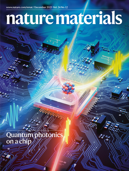
Quantum photonics on a chip
Photonic technologies enable on-chip, scalable solutions for applications in quantum communications, quantum sensing and quantum computing.
See Wang et al.
Image: Hui Wang and Chaoyang Lu, University of Science and Technology of China. Cover design: Alex Whitworth
Editorial
-
Advertisement
